Intel
®
820E Chipset
R
92 Design Guide
2.13.4. Motherboard Implementation
The following design considerations are provided for the implementation of an ICH2 platform using
AC’97. These design guidelines have been developed to ensure maximum flexibility for board designers,
while reducing the risk of board-related issues. These recommendations are not the only implementation
or a complete checklist, but they are based on the ICH2 platform.
• Components such as FET switches, buffers or logic states should not be implemented on the AC-
link signals, except for AC_RST#. Doing so would potentially interfere with timing margins and
signal integrity.
• The ICH2 supports wake-on-ring from S1-S4 states via the AC’97 link. The codec asserts
SDATAIN to wake the system. To provide wake capability and/or caller ID, standby power must be
provided to the modem codec. If no codec is attached to the link, internal pull-downs will prevent
the inputs from floating, so external resistors are not required. The ICH2 does not wake from the S5
state via the AC’97 link.
• PC_BEEP should be routed through the audio codec. Care should be taken to avoid the introduction
of a pop when powering the mixer up or down.
2.14. USB
2.14.1. Using Native USB Interface
The following are general guidelines for the USB interface:
• Unused USB ports should be terminated with 15K pull-down resistors on both P+/P- data lines.
• 15 ohm series resistors should be placed as close as possible to the ICH2 (<1 inch). These series
resistors are required for source termination of the reflected signal.
• An optional 47 pF cap may be placed as close to the USB connector as possible on the USB data
lines (P0+/-, P1+/-, P2+/-, P3+/-). This cap can be used for signal quality (rise/fall time) and to help
minimize EMI radiation.
• 15K +/-5% pull-down resistors should be placed on the USB Connector side of the series resistors
on the USB data lines (P0+/- … P3+/-), and are REQUIRED for signal termination by USB
specification. The length of the stub should be as short as possible.
• The trace impedance for the P0+/-… P3+/- signals should be 45 ohms (to ground) for each USB
signal P+ or P-. Using the stackup recommended in section 6.1, USB requires 9 mils traces. The
impedance is 90 Ω between the differential signal pairs P+ and P- to match the 90 Ω USB twisted
pair cable impedance. Note that twisted pair characteristic impedance of 90 o Ω is the series
impedance of both wires, resulting in an individual wire presenting a 45 Ω impedance. The trace
impedance can be controlled by carefully selecting the trace width, trace distance from power or
ground planes, and physical proximity of nearby traces.
USB data lines must be routed as critical signals. The P+/P- signal pair must be routed together,
parallel to each other on the same layer, and not parallel with other non-USB signal traces to
minimize crosstalk. Doubling the space from the P+/P- signal pair to adjacent signal traces will help
to prevent crosstalk. Do not worry about crosstalk between the two P+/P- signal traces. The P+/P-
signal traces must also be the same length. This will minimize the effect of common mode current
on EMI. Lastly, do not route over plane splits.
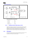
Figure 56 is the recommended USB schematic:


