Intel
®
820E Chipset
R
42 Design Guide
Table 4. Copper Tab Area Calculation
Dielectric
Thickness
(D)
Separation between
Signal Trace and
Copper Tab
Min.
Ground
Flood
Air Gap
between Signal
and GND Flood
Compensating
Capacitance
(pF)
Copper Tab
(C-TAB) Area
(A) (sq. mils)
C-TAB
Shape
(mils)
4.5 6 10 6 0.65 2800 140 L x 20 W
70 L x 40 W
Based on Equation 1, the tab area is 2800 sq. mils, where ε
r
is 4.2 and D is 4.5. These values are based
on 2116 prepreg material.
Note that more than one copper tab shape may be used. The tab dimensions are based on the copper area
over the ground plane. The actual length and width of the tabs may differ as a result of routing
constraints (e.g., if the tab must extend to center of hole, or antipad). However, each copper tab should
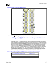
have the equivalent area. For example, the copper tabs in Figure 21 have the following dimensions, when
measured tangentially to the antipad:
Inner C-TAB = 140 (length) × 20 (width)
Outer C-TAB = 70 (length) × 40 (width)
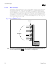
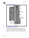
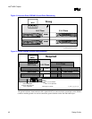
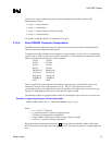
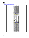
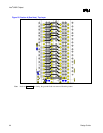
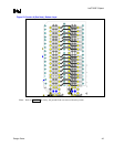
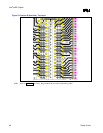
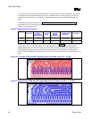
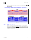
Figures 21 through 25 show a routing example of tab compensation capacitors. Note that ground floods
around the RIMM pins must not be interrupted by the capacitor tabs, and they must be connected to
avoid discontinuity in the ground plane, as shown.


