Intel
®
820E Chipset
R
78 Design Guide
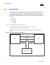
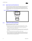
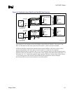
2.10.1. System Bus Ground Plane Reference
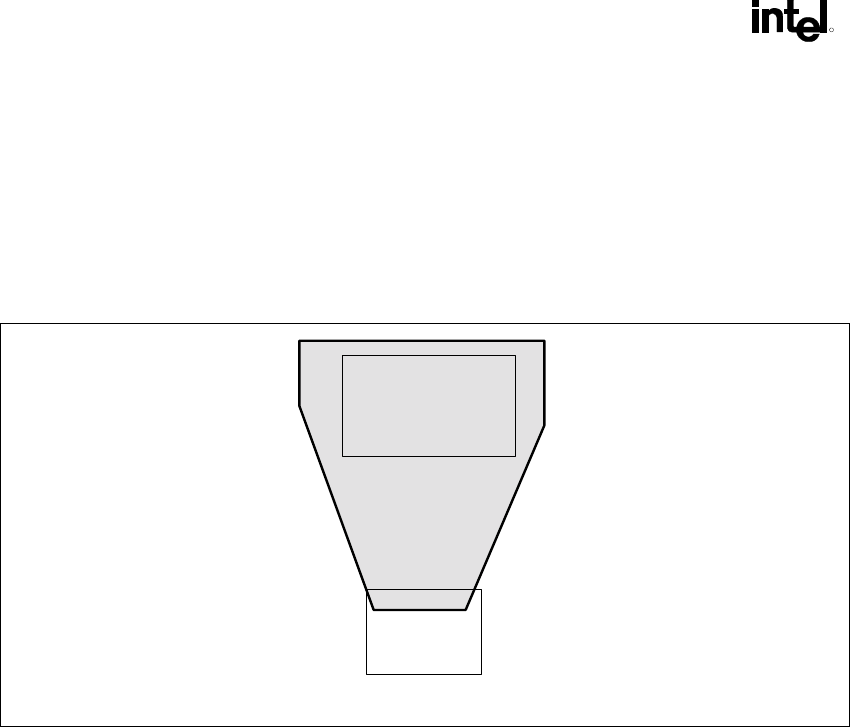
All system bus signals must be referenced to GND to provide the optimal current return path. The ground
reference must be continuous from the MCH to the Intel PGA370 socket. This may require a GND
reference island on the plane layers closest to the signals. Any split in the ground island will provide a
suboptimal return path. In a 4-layer board, this will require that the VCCID island be on an outer signal
layer. The following figure shows a 4-layer motherboard power plane with ground reference for system
bus signals.
Figure 45. Ground Plane Reference (4-Layer Motherboard)
MCH
PGA370
GND Plane
gnd_plane_ref_4layer
2.11. Additional Host Bus Guidelines
Minimizing Crosstalk on the AGTL+ Interface
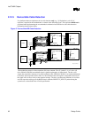
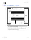
The following general rules will minimize the effect of crosstalk in a high-speed AGTL+ bus design:
• Maximize the space between traces. Maintain a minimum of 0.010 inch between traces, wherever
possible. It may be necessary to use tighter spacings when routing between component pins.
• Avoid parallelism between signals on adjacent layers.
• Since AGTL+ is a low-signal-swing technology, it is important to isolate AGTL+ signals from other
signals by at least 0.025 inch. This will avoid coupling from signals with larger voltage swings, such
as 5 V PCI.
• Select a board stack-up that minimizes the coupling between adjacent signals.
• Route AGTL+ address, data, and control signals in separate groups, to minimize crosstalk between
groups. The Pentium III processor in the FC-PGA package uses a split-transaction bus. In a given
clock cycle, the address lines and corresponding control lines could be driven by a different agent
than the data lines and their corresponding control lines.


