Intel
®
820E Chipset
R
Design Guide 171
For line section D (DRCG to last RIMM), the CTM/CTM# must be length-matched within ±2 mils.
(Exact matching is recommended.) For section C, ±2 mil trace length matching is required for the
CFM/CFM# signals.
Note: The total trace length matching for the entire CTM/CTM# signal trace (sections A+B+D) and for the
CFM/CFM# signal trace (sections A+B) is ±2 mils. (Exact length matching is recommended.)
Figure 91. Differential Clock Routing Diagram (Sections A, C & D)
Ground CLOCK CLOCK# Ground
Ground/Power Plane
22 mils 22 mils14 mils 14 mils
6 mils 6 mils6 mils
4.5 mils 4.5 mils
2.1 mils
1.4 mils
diff_clk_routing
Figure 92. Non-Differential Clock Routing Diagram (Section B)
Ground CLOCK/CLOCK# Ground
Ground/Power Plane
10 mils 10 mils18 mils
6 mils 6 mils
4.5 mils 4.5 mils
2.1 mils
1.4 mils
non-diff_clk_routing
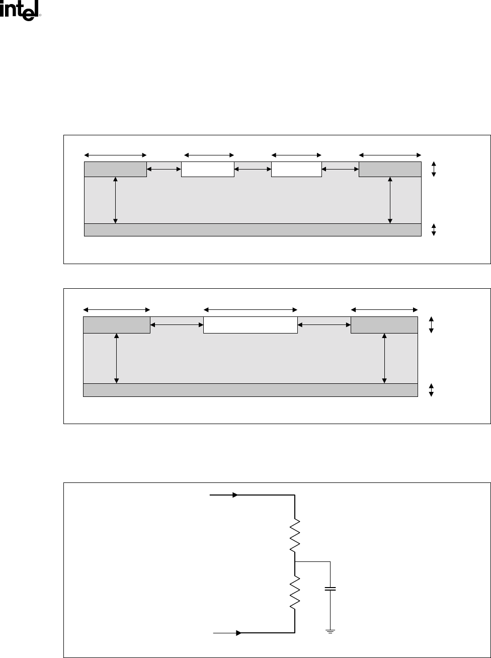
The CFM/CFM# differential pair signals require termination using either 27 Ω, 1% or 28 Ω, 2% resistors
and a 0.1 µF capacitor, as shown in the following figure.
Figure 93. Termination for Direct RDRAM* Clocking Signals CFM/CFM#
rambus_clk_term
R1
CFM
CFM#
R2
28
Ω
2%
or
27
Ω
1%
C1
0 .1 µF
28
Ω
2%
or
27
Ω
1%


