Intel
®
820E Chipset
R
174 Design Guide
4.7. Unused Outputs
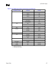
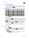
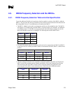
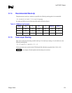
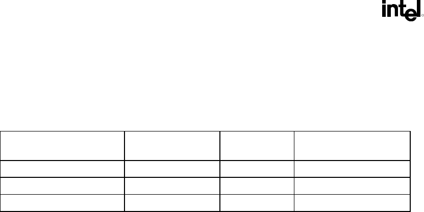
All unused clock outputs must be tied to ground through a series resistor that has approximately the
impedance of the output buffer (shown in the following table). These resistors are designed to terminate
unused outputs to eliminate EMI.
Table 60. Unused Output Termination
Buffer Name V
CC
Range
(V)
Impedance
(Ω
ΩΩ
Ω)
If Unused Output
Termination to V
ss
(Ω
ΩΩ
Ω)
CPU, CPU_Div2, IOAPIC 2.375 – 2.625 13.5 – 45 30
48 MHz, REF 3.135 – 3.465 20 – 60 40
PCI, 3V66 3.135 – 3.465 12 – 55 33
4.8. Decoupling Recommendation for CK133 and DRCG
Some CK133 vendors may integrate the XTAL_IN and XTAL_OUT frequency adjust capacitors.
However, pads should be placed on the board for these external capacitors for testing/debug.
To further reduce jitter and voltage supply noise, it is advisable to add a ferrite filter with 2 caps (10 µF
and 0.1 µF) on both the 2.5 V and 3.3 V planes, close to the clock devices. This applies to both DRCG
and CK133.


