Intel
®
820E Chipset
R
164 Design Guide
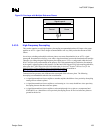
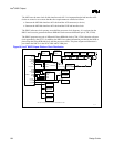
The MCH uses the same clock for hub interface and AGP. It is important that the hub interface/AGP
clocks are routed so as to ensure that the skew requirements are satisfied as follows:
• Between the MCH hub interface/AGP clock and the AGP connector (or device)
• Between the MCH hub interface/AGP clock and the ICH2 hub interface clock
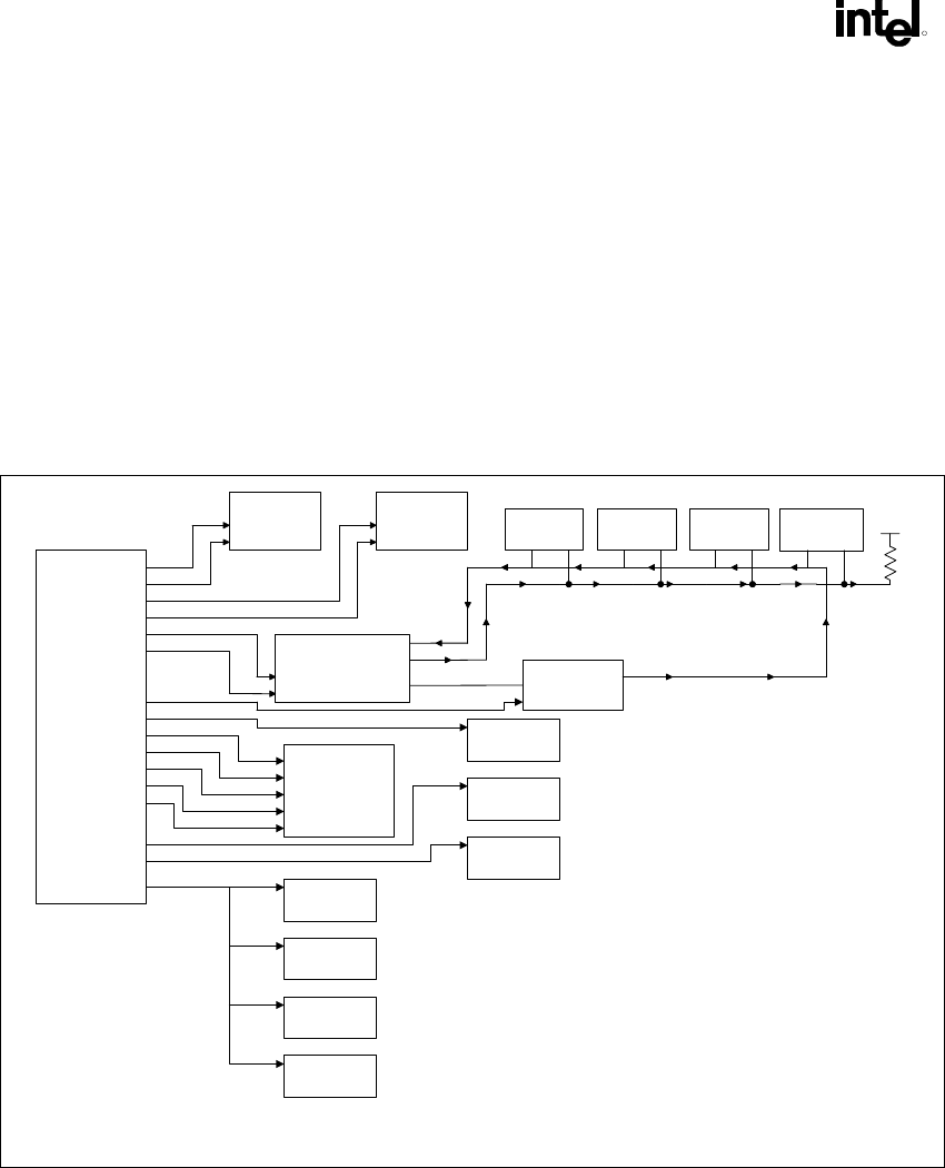
The DRCG reference clock operates at one-half the processor clock frequency. It is an input into the
DRCG and is used to generate the Direct RDRAM clock-to-master differential pair (CTM, CTM#).
The DRCG generates one pair of differential Direct RDRAM clocks (CTM, CTM#) from the reference
clock generated by the CK133. In addition, the DRCG uses phase information provided by the MCH to
phase-align the Direct RDRAM clock with the processor clocks. This phase alignment information is
provided to the DRCG via the SYNCLKN and PCLKM pins.
Figure 86. Intel
®
820E Chipset Platform Clock Distribution
CPUCLK
APIC
PCICLK*
REF
48Hz
Processor
CLK
PICCLK
Processor
CLK
PICCLK
CPUCLK
APIC
MCH
CPUCLK
HCLKIN
3V66
CLK66
RDRAM RDRAMRDRAM
CTM
CFM
RCLK TCLK
RCLKRCLK TCLK TCLK
PHASEINFO
PHASEINFO
DRCG
TERM
ICH
APIC
CPU_DIV2
REFCLK
3V66
CLK
AGP
CONNECTOR
APICCLK
PCICLK
3V66
CLK66
CLK14
CLK48
LPC
Flash BIOS
PCICLK
CLK
CLK
LPC
PCICLK
P
M
N
E
D
C
B
A
H
G
F
J
I
K
PCI SLOTS
PCI SLOTS
PCI SLOTS
PCICLK
CLK
CLK
CLK
L
L
L
CK133
Q
PCI SLOTS
CLK
L
RDRAM
RCLK TCLK
* The free-running PCI clock should be connected to the ICH.
clock_dist


