Intel
®
820E Chipset
R
156 Design Guide
3.4.2. Effective Impedance and Tolerance/Variation
The impedance of the PCB must be controlled when the PCB is fabricated. The best impedance control
specification method for each situation must be determined. The use of stripline transmission lines
(where the trace is between two reference planes) is likely to yield better results than microstrip (where
the trace is on an external layer, using an adjacent plane for reference, with solder mask and air on the
other side of the trace). This is due partly to the difficulty of precisely controlling the dielectric constant
of the solder mask as well as the difficulty of limiting the plated thickness of microstrip conductors,
which can substantially increase crosstalk.
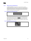
The recommended effective line impedance (Z
EFF
) is 60 Ω ± 15%, where Z
EFF
is defined by Equation 13.
Effective Impedance.
3.4.3. Power/Reference Planes, PCB Stack-Up, and High-Frequency
Decoupling
3.4.3.1. Power Distribution
Designs using the Pentium III processor require several different voltages. The following paragraphs
describe some effects of two common methods used to distribute the required voltages. Refer to the
Flexible Motherboard Power Distribution Guidelines for more information on power distribution.
The most conservative method of distributing these voltages is for each of them to have a dedicated
plane. If any of these planes is used as an “AC ground” reference for traces to control trace impedance on
the board, then the plane must be AC-coupled to the system ground plane. This method may require more
total layers in the PCB than other methods. Copper with a thickness of 1-ounce/ft
2
is recommended for
all power and reference planes.
A second method of power distribution is to use partial planes in the immediate area needing power, and
to place these planes on a routing layer, on an as-needed basis. These planes still must be decoupled to
ground to ensure stable voltages for the components being supplied. This method has the disadvantage of
reducing the area that can be used to route traces. These partial planes also may change the impedance of
adjacent trace layers. (For instance, the impedances may have been calculated for microstrip geometry,
and adding a partial plane on the other side of the trace layer may turn the microstrip into a stripline.)


