


Intel
®
820E Chipset
R
68 Design Guide
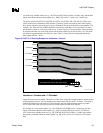
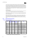
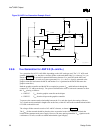
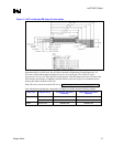
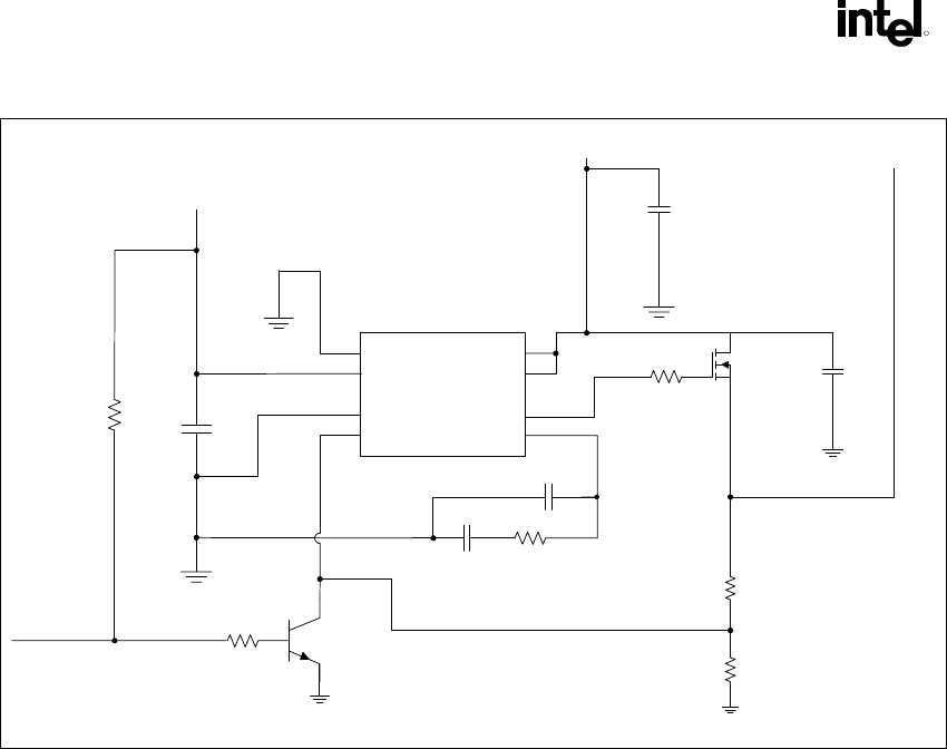
Figure 38. AGP V
DDQ
Generation Example Circuit
SHDN IPOS
VIN INEG
GND GATE
FB COMP
C1
1 k
Ω
47 µF
10 pF
7.5 k
Ω
C2
5
Ω
R3
R4
C3
O
O
O
+12V
+3.3V
VDDQ
R1
1 µF
TYPEDET#
U1
LT1575
1
2
3
4
5
6
7
8
C5
R5
C4
R2
301
Ω
1.21 k
Ω
47 µF
220 µF
agp_vddq_generation.vsd
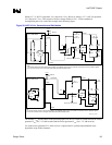
2.8.8. V
REF
Generation for AGP 2.0 (2× and 4×)
V
REF
generation for AGP 2.0 will differ, depending on the AGP card type used. The 3.3 V AGP cards
generate V
REF
locally (i.e., they have a resistor divider on the card that divides V
DDQ
down to V
REF
), as
shown in Figure 39. To account for potential differences between V
DDQ
and GND at the MCH and
graphics controller, 1.5 V cards use a source-generated V
REF
. (i.e., the V
REF
signal is generated at the
graphics controller and sent to the MCH, and another V
REF
is generated at the MCH and sent to the
graphics controller.).
Both the graphics controller and the MCH are required to generate V
REF
and distribute it through the
connector (1.5 V add-in cards only). Two pins are defined on the AGP 2.0 universal connector to allow
this V
REF
passing, as follows:
• VREFGC: V
REF
from the graphics controller to the chipset
• VREFCG: V
REF
from the chipset to the graphics controller
To preserve the common-mode relationship between the V
REF
and data signals, the routing of the two
V
REF
signals must be matched in length to the strobe lines, within 0.5 inch on the motherboard and within
0.25 inch on the add-in card.
The voltage-divider networks consist of AC and DC elements, as shown in Figure 39.
The V
REF
divider network should be placed as close as practical to the AGP interface, to obtain the
benefit of the common-mode power supply. However, the trace spacing around the V
REF
signals must be
a minimum of 25 mils, to reduce crosstalk and maintain signal integrity.