Intel
®
820E Chipset
R
48 Design Guide
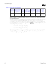
The copper tab area for the recommended stack-up was determined by means of simulation. The amount
of capacitance required is determined by the layer on which the RSL or clocking signal is routed. The
copper tabs can be placed on any signal layer, independently of the layer on which the RSL signal is
routed.
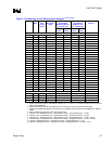
The following example calculation uses Equation 1. Approximate Copper Tab Area Calculation for a
board with an ε
r
of 4.2 and a prepreg thickness of 4.5 mils. Note that these numbers vary with the
difference in prepreg thickness.
Table 6. Copper Tab Area Calculation
Layer Dielectric
Thickness
Separation
Between
Signal Traces
& Copper Tab
Min.
Ground
Flood
Air Gap
between
Signal &
GND Flood
Compensating
Capacitance in
Cplate (pF)
CTAB Area
(sq. mils)
Top 4.5 6 10 6 0.65 – 0.85 ~2810 – 3680
Bottom 4.5 6 10 6 1.20 – 1.40 ~5194 – 6060
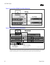
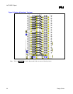
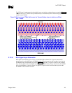
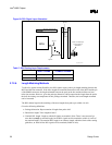
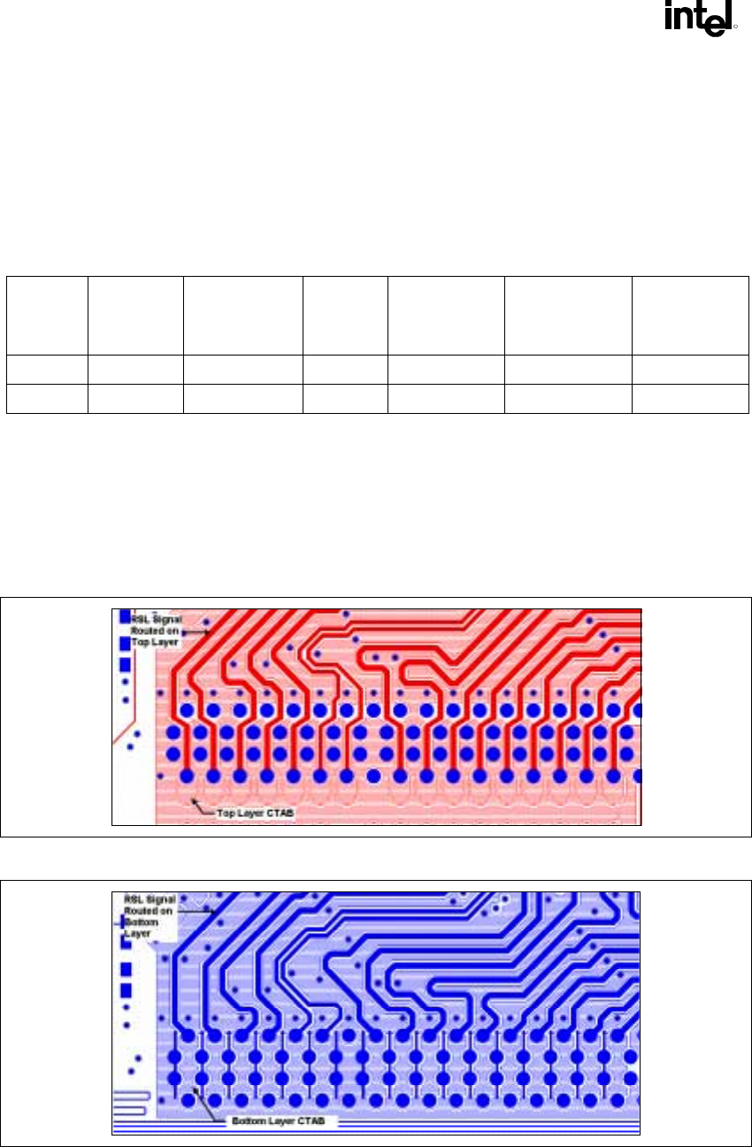
Note that more than one copper tab shape may be used, as shown in Figure 26. The dimensions are based
on the copper area over the ground plane. The actual length and width of the tabs may differ due to
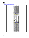
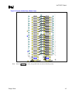
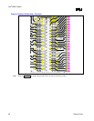
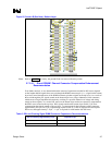
routing constraints (e.g., if tab must extend to center of hole or anti-pad). Figures 26 through 28 show a
tab compensation capacitor routing example. Note that the capacitor tabs must not interrupt ground
floods around the RIMM pins, and they must be connected, to avoid discontinuity in the ground plane, as
shown.
Figure 26. Top-Layer CTAB with RSL Signal Routed on the Same Layer (C
EFF
= 0.8 pF)
Figure 27. Bottom-Layer CTAB with RSL Signal Routed on the Same Layer (C
EFF
= 1.35 pF)


