Intel
®
820E Chipset
R
Design Guide 77
2.9.1.4. 8-Bit Hub Interface Compensation
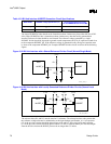
The hub interface uses a compensation signal to adjust buffer characteristics to the specific board
characteristic. The hub interface requires resistive compensation (RCOMP). The guidelines are as
follows shown in the following table.
Table 17. 8-Bit Hub Interface RCOMP Resistor Values
Component Hub Interface
Buffer Mode
Trace
Impedance
RCOMP Resistor Value RCOMP Resistor
Tied to
Normal/Single 60 Ω ± 15% 40 Ω ± 2% or 39 Ω ± 1% VCC1_8
60 Ω ± 15% 30 Ω ± 1% V
SS
ICH2
Normal/Local
50 Ω ± 10% 25 Ω ± 1% V
SS
NormalSingle 60 Ω ± 15% 40 Ω ± 2% or 39 Ω ± 1% VCC1_8
60 Ω ± 15% 30 Ω ± 1% V
SS
MCH
Normal/Local
50 Ω ± 10% 25 Ω ± 1% V
SS
The MCH also has a hub interface compensation pin. This signal (HLCOMP) also requires the RCOMP
method described for the ICH2.
2.9.1.5. 8-Bit Hub Interface Decoupling Guidelines
To improve I/O power delivery, use two 0.1 µF capacitors per component (i.e., the ICH2 and MCH).
These capacitors should be placed within 150 mils of each package, adjacent to the rows that contain the
hub interface. If the layout allows, wide metal fingers running on the V
SS
side of the board should
connect the VCC1_8 side of the capacitors to the VCC1_8 power pins. Similarly, if the layout allows,
metal fingers running on the VCC1_8 side of the board should connect the ground side of the capacitors
to the V
SS
power pins.
2.10. System Bus Design – Pentium
®
III Processor for the
Intel
®
PGA370 Socket Layout Guidelines
The Pentium III processor in the FC-PGA package is the next member of the P6 family in the
Intel
®
IA-32 processor line. The processor uses the same core and offers the same performance as the
Pentium III processor in the S.E.C.C. 2 package, but utilizes a new package technology called “Flip-Chip
Pin Grid Array,” or FC-PGA. This package utilizes the same 370-pin, zero-insertion-force socket (Intel
PGA370) used by the Intel
®
Celeron™ processor. Thermal solutions are attached directly to the back of
the processor core package, without the use of a thermal plate or heat spreader.
The Intel PGA370 design requires additional termination at the chipset for the AGTL+ signals. In
addition, the platform power delivery requirements are different for the Intel PGA370 design, compared
with the SECC2 design. The AGTL+ layout considerations detailed in Chapter 3 Advanced System Bus
Design still apply to FC-PGA designs (including ground-referencing the AGTL+ signals).
The design guidelines are found in the Intel
®
820 Chipset Design Guide Addendum for the Pentium
®
III
Processor for the PGA370 socket. These guidelines can be downloaded from the Intel website at:
http://developer.intel.com/design/chipsets/designex/298178.htm


