


Intel
®
820E Chipset
R
66 Design Guide
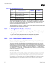
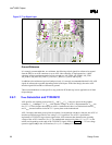
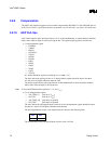
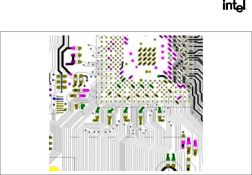
Figure 37. Top Signal Layer
Ground Reference
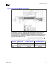
It is strongly recommended that, at a minimum, the following critical signals be referenced to ground
from the MCH to an AGP connector (or to an AGP video controller, if implemented as a “down”
solution), utilizing a minimum number of vias on each net: AD_STB0, AD_STB0#, AD_STB1,
AD_STB1#, SB_STB, SB_STB#, G_GTRY#, G_IRDY#, G_GNT#, and ST[2:0].
In addition to the minimum signal set listed previously, it is strongly recommended that half of all AGP
signals be referenced to ground, depending on the board layout. In the ideal design, the entire AGP
interface signal field would be referenced to ground.
These recommendations are not specific to any particular PCB stack-up, but are applicable to all Intel
chipset designs.
2.8.7. V
DDQ
Generation and TYPEDET#
AGP specifies two separate power planes (V
CC
and V
DDQ
). V
CC
is the core power for the graphics
controller. V
CC
is always 3.3 V. V
DDQ
is the interface voltage. In AGP 1.0 implementations, V
DDQ
was
also 3.3 V. For the designer developing an AGP 1.0 motherboard, there is no distinction between V
CC
and V
DDQ
, because both are tied to the 3.3 V power plane on the motherboard.
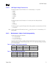
AGP 2.0 requires that these power planes be separate. In conjunction with the 4× data rate, the AGP 2.0
interface specification provides for low-voltage (1.5 V) operation. The AGP 2.0 specification
implements a TYPEDET# (type detect) signal on the AGP connector that determines the operating
voltage of the AGP 2.0 interface (V
DDQ
). The motherboard must provide either 1.5 V or 3.3 V to the
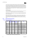
add-in card, depending on the state of the TYPEDET# signal. (Refer to Table 12.) 1.5 V low-voltage
operation applies only to the AGP interface (V
DDQ
). V
CC
is always 3.3 V.