


Intel
®
820E Chipset
R
144 Design Guide
The following two tables were derived assuming the following:
• CLK
SKEW
= 0.2 ns
Note: This assumes that clock driver pin-to-pin skew is reduced to 50 ps by tying two host clock
outputs together (“ganging”) at the clock driver output pins, and the PCB clock routing skew is
150 ps. The system timing budget must assume 0.175 ns of clock driver skew if outputs are not tied
together and a clock driver that meets the CK98 clock driver specification is being used.
• CLK
JITTER
= 0.250 ns
Some clock driver components may not support ganging the outputs. Be sure to verify with your clock
component vendor before ganging the outputs. See the appropriate Intel 820E chipset documentation for
details regarding the clock skew and jitter specifications. Refer to Section 2.7.2 and Chapter 4 for host
clock routing details.
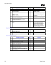
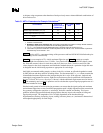
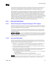
Table 52. Example T
FLT_MAX
Calculations for 133 MHz Bus
1
Driver Receiver Clk
Period
2
T
CO_MAX
T
SU_MIN
Clk
SKEW
Clk
JITTER
M
ADJ
Recommended
T
FLT_MAX
3
Processor
4
Processor
4
7.50 2.7 1.20 0.20 0.250 0.40 2.75
Processor
4
Intel
®
82820
MCH
7.50 2.7 2.27 0.20 0.250 0.40 1.68
82820 MCH Processor
4
7.50 3.63 1.20 0.20 0.25 0.40 1.82
NOTES:
1. All times in nanoseconds.
2. BCLK period = 7.50 ns @ 133.33 MHz
3. The flight times in this column include margin to account for the following phenomena that Intel has observed
when multiple bits are switching simultaneously. These multi-bit effects can adversely affect flight time and
signal quality and are sometimes not accounted for in simulation. Accordingly, maximum flight times depend on
the baseboard design and additional adjustment factors or margins are recommended.
a. SSO push-out or pull-in.
b. Rising-edge or falling-edge rate degradation at the receiver caused by inductance in the current return
path, requiring extrapolation that causes additional delay.
c. Crosstalk on the PCB and internal to the package can cause variation in the signals.
Additional effects may not necessarily be covered by the multi-bit adjustment factor and should be budgeted as
appropriate to the baseboard design. Examples include:
a. Effective board propagation constant (SEFF), which is a function of:
– Dielectric constant (
ε
r
) of the PCB material
– Type of trace connecting the components (stripline or microstrip)
– Length of the trace and load of components on trace (Note that the board propagation constant
multiplied by the trace length is a component of the flight time, but not necessarily equal to the
flight time.)
4. Processor values specified in this table are examples only. Refer to the appropriate processor datasheet for the
specification values.