


Intel
®
820E Chipset
R
Design Guide 57
2.7.5. Direct RDRAM* Clock Routing
Refer to Chapter 4 Clocking for the Intel 820E chipset platform’s Direct RDRAM clock routing
guidelines.
2.7.6. Direct RDRAM* Design Checklist
Use the following checklist as a final check to ensure that the motherboard incorporates solid design
practices. This list is only a reference. For correct operation, all of the design guidelines within this
document must be followed.
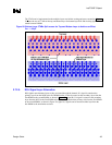
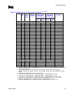
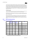
Table 9. Signal List
RSL Signals High-Speed
CMOS Signals
Serial
CMOS Signal
Clocks
• DQA[8:0]
• DQB[8:0]
• RQ[7:0]
• CMD
• SCK
• SIO • CTM
• CTM#
• CFM
• CFM#
• Ground isolation well grounded.
Via to ground every 0.5 inch around edge of isolation island
Via to ground every 0.5 inch between RIMMs
Via to ground every 0.5 inch between signals (from MCH to first RIMM)
Via between every signal within 100 mils of the MCH edge and the connector edge
No unconnected ground floods
All ground isolation at least 10 mils wide.
Ground isolation fills between serpentines
Ground isolation not broken by C-TABs.
Ground isolation connects to the ground pins in the middle of the RIMM connectors.
Ground isolation vias connect on all 4 layers and should not have thermal reliefs.
Ground pins in RIMM connector connect on all 4 layers.
• V
TERM
layout yields low noise.
Solid V
TERM
island is on top layer. Do not split this plane.
Ground island (for ground side of V
TERM
caps) is on top.
Termination resistors connect directly to the V
TERM
island on the top layer (without vias).
Decoupling V
TERM
is critical!
Decoupling capacitors connect directly to top-layer V
TERM
island and top-layer ground island.
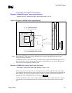
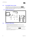
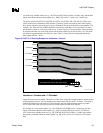
(See the layout example.)
Use at least 2 vias per decoupling capacitor in the top-layer ground island.
Use 2 × 100 µF tantalum capacitors to decouple V
TERM
. (Aluminum/electrolytic capacitors are
too slow!)
High-frequency decoupling capacitors must be spread out across the termination island so that
all termination resistors are near high-frequency capacitors.
100 µF tantalum capacitors should be at each end of the V
TERM
island.
100 µF tantalum capacitors must be connected directly to V
TERM
island.
100 µF tantalum capacitors must have at least 2 vias/cap to ground.
V
TERM
island should be 50–75 mils wide.
V
TERM
island should not be broken.