


228 AMD Geode™ LX Processors Data Book
GeodeLink™ Memory Controller Register Descriptions
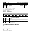
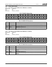
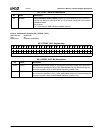
33234H
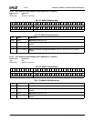
36 D0_CB DIMM0 Component Banks. Number of component banks per module bank for DIMM0.
0: 2 Component banks. (Default)
1: 4 Component banks.
35 RSVD Reserved.
34:32 D0_PSZ DIMM0 Page Size.
000: 1 KB 100: 16 KB
001: 2 KB 101: 32 KB
010: 4 KB 110: Reserved
011: 8 KB 111: DIMM0 Not Installed (Default)
31:30 RSVD Reserved.
29:28 MSR_BA Mode Register Set Bank Address. These are the bank select bits used for program-
ming the DDR DIMM’s Extended Mode Register. These bits select whether the GLMC is
programming the Mode Register or the Extended Mode Register.
00: Program the DIMM Mode Register. (Default)
01: Program the DIMM Extended Mode Register. Bits [26:24] determine the program
data.
10: Reserved.
11: Reserved.
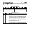
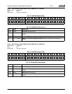
27 RST_DLL Mode Register Reset DLL. This bit represents A8 in the Mode Register, which when set
to 1 resets the DLL as part of the DIMM initialization sequence. JEDEC recommends
clearing this bit back to 0 on the final load-mode-register command before activating any
bank.
0: Do not reset DLL. (Default.
1: Reset DLL.
26 EMR_QFC Extended Mode Register FET Control. This bit programs the DIMM’s QFC# signal. The
QFC# signal provides control for FET switches that are used to isolate module loads from
the system memory busy at times when the given module is not being accessed. Only
pertains to x4 configurations.
0: Enable. (Default)
1: Disable.
25 EMR_DRV Extended Mode Register Drive Strength Control. This bit selects either normal or
reduced drive strength.
0: Normal. (Default)
1: Reduced.
24 EMR_DLL Extended Mode Register DLL. This bit disables/enables the DLL.
0: Enable. (Default)
1: Disable.
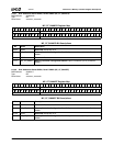
23:8 REF_INT Refresh Interval. This field determines the number of SDRAM clocks between refresh.
This value multiplied by 16 is the average number of clocks between refresh. The default
value, 00h, disables refresh.
7:4 REF_STAG Refresh Staggering. This field controls the number of clocks (0-16) between REF com-
mands to different banks during refresh cycles. Staggering is used to help reduce power
spikes during refresh. Note that with a setting of 0, no staggering occurs, so all module
banks are refreshed simultaneously. (Default = 1)
3 REF_TST Test Refresh. This bit, when set high, generates one refresh request that the GLMC
queues in its refresh request queue. Since the refresh queue is 8-deep, 8 sets/clears of
this bit queues 8 refresh requests, thus forcing a refresh request out to DRAM. This bit
should only be used for initialization and test. (Default = 0)
MC_CF07_DATA Bit Descriptions (Continued)
Bit Name Description