


AMD Geode™ LX Processors Data Book 307
Display Controller Register Descriptions
33234H
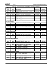
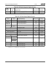
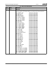
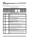
40 SEQIOR_SMI Sequencer Register Read SMI. Reading a 1 indicates that one or more of the VGA’s
Sequencer registers has been read; writing a 1 to this bit clears it.
39 SEQIOW_SMI Sequencer Register Write SMI. Reading a 1 indicates that one or more of the VGA’s
Sequencer registers has been written; writing a 1 to this bit clears it.
38 CRTCIOR_SMI CRTC Register Read SMI. Reading a 1 indicates that one or more of the VGA’s CRTC
registers has been read; writing a 1 to this bit clears it.
37 CRTCIOW_SMI CRTC Register Write SMI. Reading a 1 indicates that one or more of the VGA’s CRTC
registers has been written; writing a 1 to this bit clears it.
36 CRTCIO_SMI CRTC Invalid Register I/O SMI. Reading a 1 indicates that this SMI has been gener-
ated; writing a 1 to this bit clears it; writing 0 has no effect.
35 VGA_BL_SMI VGA Vertical Blank SMI. Reading a 1 indicates that the ASMI corresponding to VGA
Vertical Blank has been triggered. Writing a 1 to this bit clears it (and deactivates the
ASMI signal); writing a 0 to this bit has no effect.
34 ISR0_SMI Input Status Register 0 SMI. Reading a 1 indicates that a synchronous SMI was gen-
erated because of a read to VGA Input Status Register 0. Writing a 1 to this bit clears it;
writing a 0 has no effect.
33 MISC_SMI Miscellaneous Output Register SMI. Reading a 1 indicates that a synchronous SMI
was generated due to a write to the Miscellaneous Output Register. Writing a 1 to this
bit clears it; writing a 0 has no effect.
32 VG_BL_SMI DC Vertical Blank SMI. Reading a 1 indicates that the ASMI corresponding to DC Ver-
tical Blank has been triggered. Writing a 1 to this bit clears it (and deactivates the ASMI
signal); writing a 0 has no effect.
31:29 RSVD Reserved. Set to 0.
28 VGA_RES_
CHANGE_MASK
VGA Resolution Change SMI Mask. When set to 1, disables generation of an asyn-
chronous SMI when all of the following conditions occur at once:
- The VGA timing engine is enabled.
- Scaling is enabled.
- The horizontal or vertical resolution of the image produced by the VGA timing engine
changes.
27:17 RSVD Reserved. Set to 0.
16 ISR1R_MSK Input Status Register 1 Read SMI Mask. When set to 1, disables generation of the
SMI that indicates that VGA Input Status Register 1 has been read.
15 MSICIOR_MSK Miscellaneous Output Register Read SMI. When set to 1, disables generation of the
SMI that indicates that the VGA Miscellaneous Output Register has been read.
14 DACIOR_MSK Video DAC Register Read SMI. When set to 1, disables generation of the SMI that
indicates that one or more of the VGA’s Video DAC registers has been read.
13 DACIOW_MSK Video DAC Register Write SMI. When set to 1, disables generation of the SMI that
indicates that one or more of the VGA’s Video DAC registers has been written.
12 ATRIOR_MSK Attribute Register Read SMI. When set to 1, disables generation of the SMI that indi-
cates that one or more of the VGA’s Attribute registers has been read.
11 ATRIOW_MSK Attribute Register Write SMI. When set to 1, disables generation of the SMI that indi-
cates that one or more of the VGA’s Attribute registers has been written.
10 GFXIOR_MSK Graphics Controller Register Read SMI. When set to 1, disables generation of the
SMI that indicates that one or more of the VGA’s Graphics Controller registers has
been read.
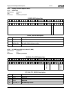
GLD_MSR_SMI Bit Descriptions (Continued)
Bit Name Description