314 AMD Geode™ LX Processors Data Book
Display Controller Register Descriptions
33234H
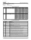
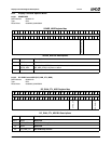
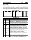
6.6.3.2 DC General Configuration (DC_GENERAL_CFG)
This register contains general control bits for the DC. Unless otherwise noted in the bit descriptions table, settings written to
this register do not take effect until the start of the following frame or interlaced field.
DC Memory Offset 004h
Typ e R /W
Reset Value 00000000h
DC_GENERAL_CFG Register Map
313029282726252423222120191817161514131211109876543210
DBUG
DBSL
CFRW
DIAG
CRC_MODE
SGFR
SGRE
SIGE
SIG_SEL
FRC8PIX
RSVD
YUVM
VDSE
VGAFT
FDTY
STFM
DFHPEL DFHPSL
VGAE
DECE
CMPE
FILT_SIG_SEL
VIDE
CLR_CUR
CURE
DFLE
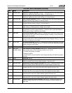
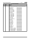
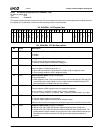
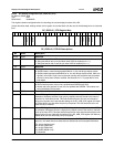
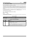
DC_GENERAL_CFG Bit Descriptions
Bit Name Description
31 DBUG Debug Mode. Effective immediately.
0: Disable
1: Enable.
30 DBSL Debug Select. Effective immediately.
0: FIFO control signals transmitted to debug port.
1: Memory control signals transmitted to debug port.
29 CFRW Compressed Line Buffer Read/Write Select. Effective immediately.
Only has effect if in DIAG mode (bit 28 = 1).
0: Write address enabled to Compressed Line Buffer (CLB) in diagnostic mode.
1: Read address enabled to CLB in diagnostic mode.
28 DIAG RAM Diagnostic Mode. Effective immediately.
0: Normal operation.
1: RAM diagnostic mode. This bit allows testability of the on-chip Display FIFO and CLB
via the diagnostic access registers. A low to high transition resets the Display FIFO
and Compressed Line Buffer read and write pointers.
27 CRC_MODE CRC Mode. Effective immediately.
This bit selects the CRC algorithm used to compute the signature.
0: nxt_crc[23:0] <= {crc[22:0], (crc[23], crc[3], crc[2])} ^ data[23:0].
1: nxt_crc = (reset) ? 32’h01 :( {crc[30:0], 1’b0} ^ ((crc[31]) ? 32’h04c11db7 : 0) )^ data.
26 SGFR Signature Free Run. Effective immediately.
0: Capture display signature for one frame.
1: Capture display signature continuously for multiple frames.
When this bit is cleared, the signature accumulation stops at the end of the current frame.
25 SGRE Signature Read Enable. Effective immediately.
0: Reads to DC_PAL_DATA (DC Memory Offset 074h[23:0]) return palette data.
1: Reads to DC_PAL_DATA (DC Memory Offset 074h[23:0]) return signature data. The
palette address register contents are ignored in this case. Note that the automatic pal-
ette address increment mechanism will still operate even though the address is
ignored.


