AMD Geode™ LX Processors Data Book 337
Display Controller Register Descriptions
33234H
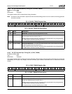
6.6.7.4 DC Compression FIFO Diagnostic (DC_CFIFO_DIAG)
This register is provided to enable testability of the compressed line buffer (FIFO) RAM. Before it is accessed, the DIAG bit
should be set high (DC Memory Offset 004h[28] = 1) and the DFLE bit should be set low (DC Memory Offset 004h[0] = 0).
Also, the CFRW bit in DC_GENERAL_CFG (DC Memory Offset 004h[29]) should be set appropriately depending on
whether a series of reads or writes is to be performed. After each write, the FIFO write pointer automatically increments.
After all write operations are performed, the CFRW bit should be set high to enable read addresses to the FIFO and a pair
of reads of don't care data should be performed to load 64 bits of data into the output latch. Each subsequent read contains
the appropriate data that was previously written. After each pair of reads, the FIFO read pointer automatically increments.
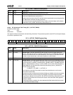
DC Memory Offset 07Ch
Typ e R /W
Reset Value xxxxxxxxh
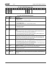
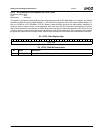
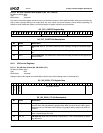
DC_CFIFO_DIAG Register Map
313029282726252423222120191817161514131211109876543210
CFIFO_DATA
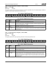
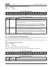
DC_CFIFO_DIAG Bit Descriptions
Bit Name Description
31:0 CFIFO_DATA Compressed Data FIFO Diagnostic Read or Write Data.


