AMD Geode™ LX Processors Data Book 453
Video Processor Register Descriptions
33234H
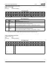
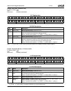
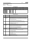
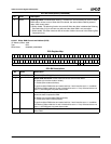
6.8.3.44 Panel Timing Register 2 (PT2)
VP Memory Offset 408h
Typ e R /W
Reset Value 00000000_00000000h
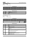
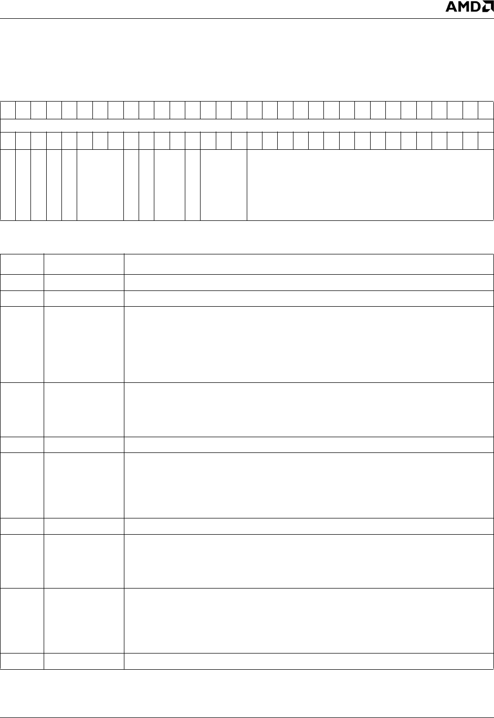
PT2 Register Map
63 62 61 60 59 58 57 56 55 54 53 52 51 50 49 48 47 46 45 44 43 42 41 40 39 38 37 36 35 34 33 32
RSVD
313029282726252423222120191817161514131211109876543210
SP
TFT_PASS_THRU
LPOL
RSVD
SCRC
RSVD
VSP
HSP
RSVD
MCS
PIXF RSVD
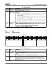
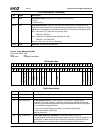
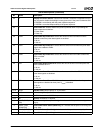
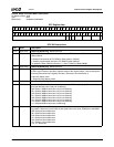
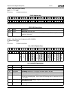
PT2 Bit Descriptions
Bit Name Description
63:32 RSVD (RO) Reserved (Read Only). Reads back as 0.
31 SP Spare. Bit is read/write, but has no function.
30 TFT_PASS_
THRU
TFT Pass Through. Activates the TFT Pass Through mode. In TFT Pass Through
mode, the input timing and the pixel data is passed directly on to the panel interface tim-
ing and the panel data pins to drive the TFT panel. In Pass Through mode the internal FP
TFT logic and timing is not used.
0: Normal mode; uses the TFT logic and timing from the FP.
1: TFT Pass Through mode; FP TFT timing logic functions are not used.
29 LPOL Display Timing Strobe Polarity Select. Selects the polarity of the LDE/MOD pin. This
can be used for panels that require an active low timing LDE interface signal.
0: LDE/MOD signal is active high. (Default)
1: LDE/MOD signal is active low
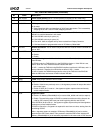
28 RSVD Reserved. This bit is not defined.
27 SCRC Panel Shift Clock Retrace Activity Control. Programs the shift clock (SHFCLK) to be
either free running, or active only during the display period. Some TFT panels recom-
mend keeping the shift clock running during the retrace time.
0: Shift clock is active only during active display period.
1: Shift clock is free running during the entire frame period.
26:24 RSVD Reserved. These bits are not defined.
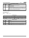
23 VSP Vertical Sync Output Polarity. Selects polarity of the output VSYNC signal. Note that
VP Memory Offset 400h[30] selects the polarity of the input VSYNC.
0: VSYNC output is active high.
1: VSYNC output is active low
22 HSP Horizontal Sync Output Polarity. Selects polarity of output HSYNC signal. Note that
VP Memory Offset 400h[29] selects the polarity of the input HSYNC, and this bit controls
the output polarity.
0: HSYNC output is active high.
1: HSYNC output is active low
21:20 RSVD Reserved. These bits are not defined.


