AMD Geode™ LX Processors Data Book 491
Video Input Port Register Descriptions
33234H
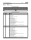
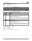
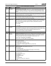
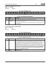
26 ANCPEN Ancillary Parity Check Enable. When set to 1, ancillary DID, SDID, NN, and check sum
bytes are checked for even parity. The error is reported on MSR 4002002h[23]. When
this bit is 0, the Ancillary Checksum or Parity Error bit only indicates ancillary checksum
errors.
25 LPB VOP to VIP Loopback. When set to 1, the VOP clock and data are used as the clock
and data inputs to the VIP. This allows for loopback testing of the VOP and VIP functions.
This bit must be set to 0 for normal VIP operation.
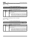
24 FF_R/W FIFO R/W Enable. When set to 1, the FIFO Address (VIP Memory Offset 70h) and FIFO
Data (VIP Memory Offset 74h) registers can be used to write and read the 256x32 bit
FIFO. This bit must be set to 0 for normal VIP operation.
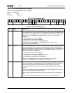
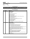
23:21 PAGE_CNT Page Count. Determines how many pages of video data are used. When this value is
000, a single page of video data is stored (Default). Additional pages are saved by add-
ing the value in the Page Offset register (VIP Memory Offset 68h) to each base.
000: 1 Page. (Default)
001: 2 Pages.
“
111: 8 Pages.
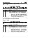
20:16 ANC_FF_
THRESH
Ancillary FIFO Threshold. Watermark level for setting the ancillary FIFO threshold. This
value also determines when the secondary priority is used during a write request. If the
FIFO WORD count exceeds this value, the secondary priority ID is used. An INT or SMI
can also be generated if this threshold is exceeded. Threshold value. 0-31.
The Ancillary FIFO depth is always 64 QWORDs.
15 RSVD Reserved.
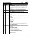
14:8 VID_FF_
THRESH
Video FIFO Threshold. Watermark level for setting the video FIFO threshold. This value
also determines when the secondary priority is used during a write request. If the FIFO
WORD count exceeds this value, the secondary priority ID is used. An INT or SMI can
also be generated if this threshold is exceeded. Threshold value. 0-127
Linear mode: Y buffer depth is 192 QWORDs.
Planar mode: Y,U,V buffer depths are all 64 QWORDs
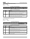
7:5 SYNC_TO_PIN Sync Select. Selects signal timing for VIP_VSYNC pin.
000: 0 (output disabled).
001: Select vsync_in from DC.
010: Select vsync_in from DC (inverted).
011: Select bit 17 of Status register (VIP Memory Offset 08h).
100-111: 0.
4:3 FIELD_TO_DC Field to DC Select. Selects signal for field_to_vg.
00: Field input.
01: Inverted field input.
10: LSB of page being written (indicates which page is currently active).
11: Inverted LSB of page being written.
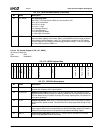
2:0 SYNC_TO_DC VSYNC Select. Selects signal timing for VIP_VSYNC output to the DC.
000: Sync from pin.
001: Inverted sync from pin.
010: VBLANK.
011: Inverted VBLANK.
100: Field.
101: Inverted field.
110: When vip_current_line = target_line.
111: 0.
VIP_CTL_REG2 Bit Descriptions (Continued)
Bit Name Description


