


322 AMD Geode™ LX Processors Data Book
Display Controller Register Descriptions
33234H
6.6.4.2 DC Compression Buffer Start Address (DC_CB_ST_OFFSET)
This register specifies the offset at which the compressed display buffer starts. Settings written to this register do not take
effect until the start of the following frame or interlaced field.
6.6.4.3 DC Cursor Buffer Start Address (DC_CURS_ST_OFFSET)
This register specifies the offset at which the cursor memory buffer starts. Settings written to this register do not take effect
until the start of the following frame or interlaced field.
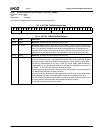
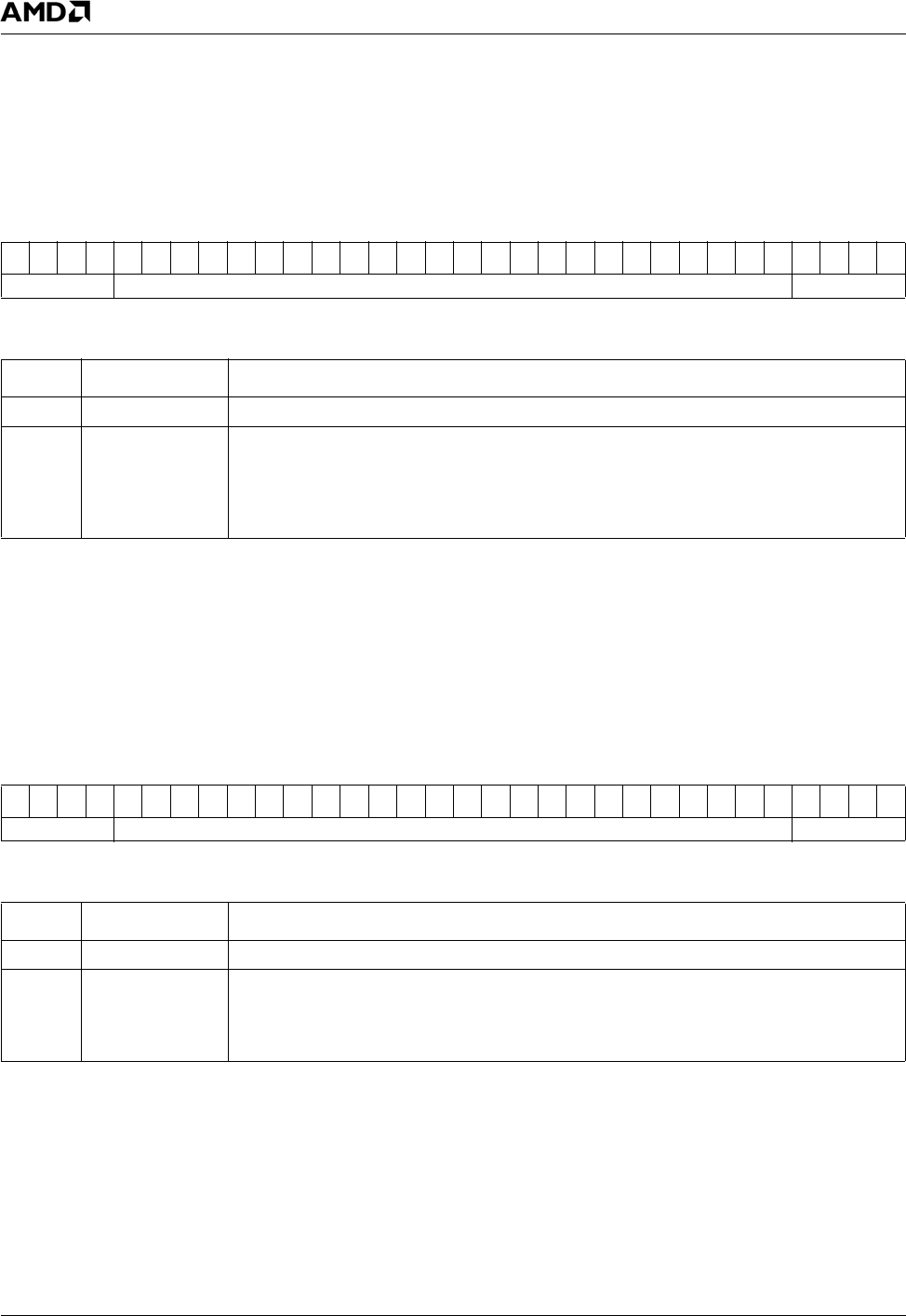
DC Memory Offset 014h
Typ e R /W
Reset Value xxxxxxxxh
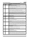
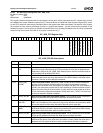
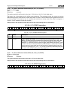
DC_CB_ST_OFFSET Register Map
313029282726252423222120191817161514131211109876543210
RSVD OFFSET 0h
DC_CB_ST_OFFSET Bit Descriptions
Bit Name Description
31:28 RSVD Reserved.
27:0 OFFSET Compressed Display Buffer Start Offset. This value represents the byte offset of the
starting location of the compressed display buffer. The lower five bits should always be
programmed to zero so that the start offset is aligned to a 32-byte boundary. This value
should change only when a new display mode is set due to a change in size of the frame
buffer.
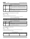
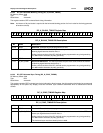
DC Memory Offset 018h
Typ e R /W
Reset Value xxxxxxxxh
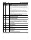
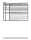
DC_CURS_ST_OFFSET Register Map
313029282726252423222120191817161514131211109876543210
RSVD OFFSET 0h
DC_CURS_ST_OFFSET Bit Descriptions
Bit Name Description
31:28 RSVD Reserved.
27:0 OFFSET Cursor Start Offset. This value represents the byte offset of the starting location of the
cursor display pattern. The lower five bits should always be programmed to zero so that
the start offset is 32-byte aligned. Note that if there is a Y offset for the cursor pattern, the
cursor start offset should be set to point to the first displayed line of the cursor pattern.