356 AMD Geode™ LX Processors Data Book
Display Controller Register Descriptions
33234H
6.6.17 VGA Block Standard Registers
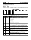
6.6.17.1 VGA Miscellaneous Output
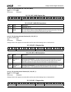
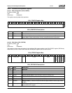
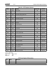
2 VBLANK_SMI VBLANK SMI. If = 1, an SMI was generated due to leading edge vertical blank.
1 ISR0_SMI Input Status Register 0 SMI. If = 1, an SMI was generated from an I/O IN to Input Status
Register 0.
0MISC_SMI Miscellaneous Output Register SMI. If = 1, an SMI was generated from an I/O OUT to
the Miscellaneous Output Register.
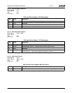
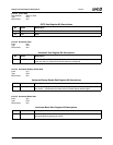
Read Address 3CCh
Write Address 3C2h
Typ e R /W
Reset Value 02h
VGA_STATUS Bit Descriptions (Continued)
Bit Name Description
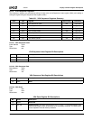
VGA Miscellaneous Output Register Bit Descriptions
Bit Name Description
7 VSYNC_POL Vertical Sync Polarity. Selects a positive-going VSYNC pulse (bit = 0) or a negative-
going VSYNC pulse (bit = 1).
6 HSYNC_POL Horizontal Sync Polarity. Selects a positive-going HSYNC pulse (bit = 0) or a negative-
going HSYNC pulse (bit = 1).
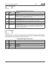
5PAGE Page Bit. This bit is used to replace memory address bit A0 as the LSB when bit 1 of the
Miscellaneous register (Index 06h[1]) in the VGA Graphics Controller is set to 1.
4 RSVD Reserved.
3:2 CLK_SEL Clock Select. Selects the VGA pixel clock source. Writes to this register will directly
affect the frequency generated by the Dot clock PLLs. The value of this register is sam-
pled when it is written; The Dot clock frequency can be overridden by subsequent writes
to the Dot clock PLL controls. If the VGA is disabled or in fixed timing mode, the Dot clock
frequency is NOT affected by writes to this register.
00: Selects clock for 640/320 pixels per line (25.175 MHz Dot clock).
01: Selects clock for 720/360 pixels per line (28.325 MHz Dot clock).
10: Reserved.
11: Reserved.
1RAM_EN RAM Enable. Enables the video frame buffer address decode when set to 1.
0 ID_ADDR_SEL I/O Address Select. Determines the I/O address of the CRTC Index and Data registers
(Index 3?4h and 3?5h), Feature Control register (Index 3?Ah), and Input Status Register
1 (Index 3?Ah) as follows: ? = B when bit set to 0 (MDA I/O address emulation), ? = D
when bit set to 1 (CGA address emulation).


