


614 AMD Geode™ LX Processors Data Book
Electrical Specifications
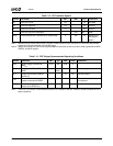
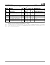
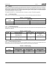
33234H
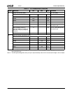
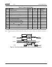
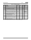
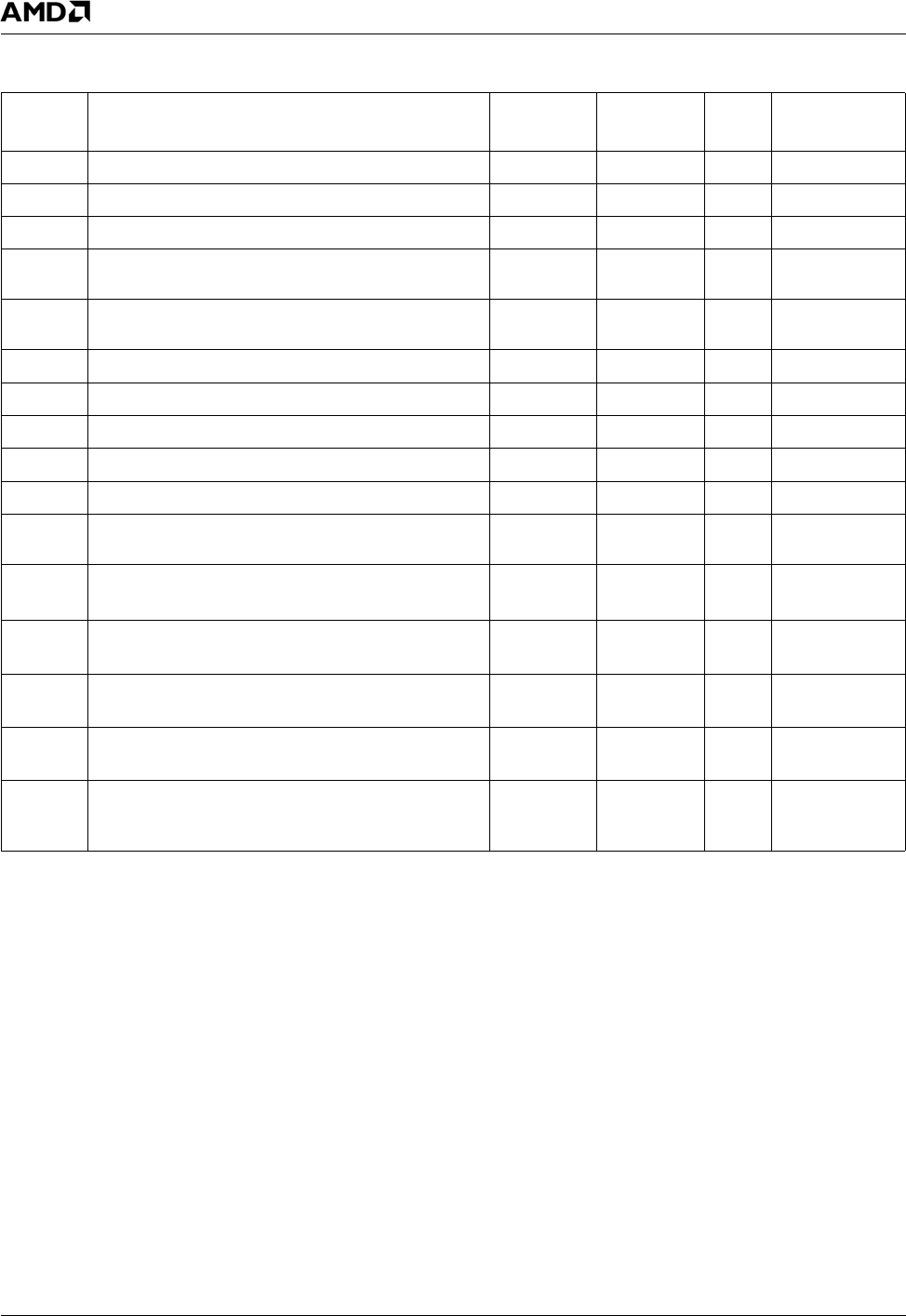
Table 7-15. Memory (DDR) Interface Signals
Symbol
(Note 1) Parameter Min Max Unit Comments
t
CK
SDCLK[5:0]P, SDCLK[5:0]N period 5.0 ns Note 2
t
CH
SDCLK[5:0]P, SDCLK[5:0]N High time 2.4 ns 48% t
CK
t
CL
SDCLK[5:0]P, SDCLK[5:0]N Low time 2.4 ns 48% t
CK
t
SKEW1
SDCLK[n]P to SDCLK[n]N skew (n=0..5) 0.1 ns Guaranteed by
design
t
DEL1
SDCLK[5:1]P, SDCLK[5:0]N edge delay from
SDCLK[0]P
-0.2 0.2 ns Note 2, Note 3
DQS[7:0] Input and output period 5.0 ns Same as t
CK
t
DQSCK
DQS[7:0] Input delay relative to SDCLK[5:0] -0.5 t
CK
-2 ns Note 4
t
DEL2
DQS[7:0] output edge delay from SDCLK[5:0] -0.5 0.5 ns Note 3
t
RPRE
DQS input preamble before first DQS rising edge 0.25*t
CK
ns Note 3
t
RPST
DQS input postamble after last DQS rising edge 0.25*t
CK
Note 3
t
WPRE
DQS output write preamble valid time before
SDCLK[5:0] rising edge
0.5*t
CK
-0.4 0.5*t
CK
+1 ns
t
WPST
DQS output write postamble after last DQS falling
edge
0.75*t
CK
-0.4
0.75*t
CK
+1 ns
t
DQSQs
DQ[63:0] Input setup time from DQS -0.25*t
CK
+0.5
ns Note 3,Note 5
t
DQSQh
DQ[63:0] Input hold time from DQS 0.25*t
CK
+0.5
ns Note 3, Note 5
t
VAL1
DQ[63:0], DQM[7:0] Output Data Valid Delay time
from DQS rising OR falling edge
0.25*t
CK
-0.4
0.25*t
CK
+0.4
ns Note 3,
t
VAL2
MA[12:0], BA[1:0], CAS[1:0]#, RAS[1:0]#,
CKE[1:0], CS[3:0]#, WE[1:0] Output Valid Delay
time from SDCLK[5:0]
1.1 3.0 ns Note 3, Note 4
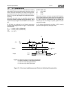
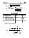
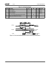
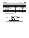
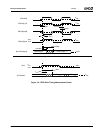
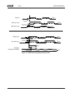
Note 1. Refer to Figure 7-8 "DDR Write Timing Measurement Points" on page 615 and Figure 7-9 "DDR Read Timing Mea-
surement Points" on page 616.
Note 2. The SDCLKP and SDCLKN clocks are inversions of each other (differential clocking).
Note 3. These parameters guarantee device timing, but they may be tested to a looser value to allow for tester uncertain-
ties. Devices that meet the loosened tester values meet specs when correlated with lab measurements.
Note 4. t
VAL2
and t
DQSCK
timings are achieved for different DIMM loadings by proper initial settings of the
GLCP_DELAY_CONTROLS MSR. Typical tester results with clock and address loaded equally and no pro-
grammed delay for address are 0 ns for t
VAL2
.
Note 5. The DQ timing relative to DQS are on a per-byte basis only. DQ[7:0] and DQM[0] should be measured against
DQS[0], DQ[15:8] and DQM[1] should be measured against DQS[1], etc.