532 AMD Geode™ LX Processors Data Book
Security Block Register Descriptions
33234H
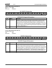
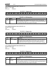
6.12.3.23 SB EEPROM Security State (SB_EEPROM_SEC_STATE)
This read only register contains the current state of the access control bits for controlling reads and writes from/to the
EEPROM. It is reloaded from the EEPROM array after every reset. The initial state of the EEPROM is all ones. Therefore
the unlocked state of the control bits must be one. The user locks the part by programming zeroes into the protect bits of the
Access Control bytes. Each lock control is a 3-bit field. The user normally programs all three bits to a zero. The multi-bit
fields are used to prevent a single bit disturb of the EEPROM array from unlocking the part.
SB Memory Offset 80Ch
Typ e RO
Reset Value 00000000h
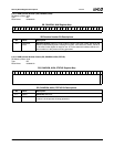
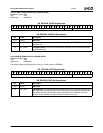
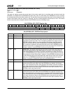
SB_EEPROM_SEC_STATE Register Map
31 30 29 28 27 26 25 24 23 22 21 20 19 18 17 16 15 14 13 12 11 10 9 8 7 6 5 4 3 2 1 0
EEPROM byte 1 EEPROM byte 0
RSVD WPE DBL RSVD WPU WPL
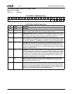
SB_EEPROM_SEC_STATE Bit Descriptions
Bit Name Description
31:14 RSVD Reserved.
13:11 WPE Write Protect Extended. Reserved for future use. This register holds the 3-bit value of
the access control bits used to block write access to any address above the 2 Kbit range
(byte address greater than 255). This is included for possible future support of larger
EEPROM memories. With the currently specified 2 Kbit memory, these bits have no
effect. If any of these bits are reset, write operations are blocked to addresses above
255. These bits correspond to the state of bits [5:3] of byte 1of the EEPROM array as
read after the last reset. To change these bits, the user must program the Access Con-
trol byte 1 (address 1 of the EEPROM), and the part must be reset.
10:8 DBL Debug Lock. This register holds the 3-bit value of the access control bits used to dis-
able certain debug features of the AMD Geode LX processor. If any of these bits are
reset, debug operations are blocked. These bits correspond to the state of bits [2:0] of
byte 1 of the EEPROM array as read after the last reset. To change these bits, the User
must program the Access Control byte 1 (address 1 of the EEPROM), and the part must
be reset. Although reset to the locked state (000), these bits will revert to the unlocked
state (111), if no EEPROM is detected after reset. This unlocking will occur approxi-
mately 17 ms after the release from reset with no EEPROM present.
7:6 RSVD Reserved.
5:3 WPU Write Protect Upper. This register holds the 3-bit value of the access control bits used
to block write access to the upper half of the EEPROM array, (address 120 through
255). If any of these bits are reset, write operations are blocked. These bits correspond
to the state of bits [5:3] of byte 0 of the EEPROM array as read after the last reset. To
change these bits, the user must program the Access Control byte 0 (address 0 of the
EEPROM), and the part must be reset.
2:0 WPL Write Protect Lower. This register holds the 3-bit value of the access control bits used
to block write access to the lower half of the EEPROM array, (address 0 through 127).
(Note, these addresses include these access control bits as well as the hidden key bits.)
If any of these bits are reset, write operations are blocked forever. These bits correspond
to the state of bits [2:0] of byte 0 of the EEPROM array as read after the last reset. To
change these bits, the user must program the Access Control byte 0 (address 0 of the
EEPROM), and the part must be reset.


