268 AMD Geode™ LX Processors Data Book
Graphics Processor Register Definitions
33234H
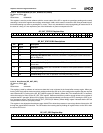
6.4.2.13 BLT Mode (GP_BLT_MODE)
Writing to this register configures the BLT mode and initiates the rendering of the BLT. If a BLT or vector operation is already
in progress when this register is written, the BLT pending bit in GP_BLT_STATUS (GP Memory Offset 44h) is set and the
BLT is queued to begin when the current operation is complete. Software should not write to any register (other than
GP_HOST_SRC if required) while the BLT pending bit is set since it will corrupt the pending BLT. Setting the TH bit causes
the BLT operation to wait until the next VBLANK before beginning. Software may still queue another operation behind a
throttled BLT as long as the BLT pending bit is clear.
GP Memory Offset 40h
Typ e WO
Reset Value 00000000h
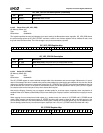
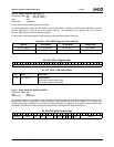
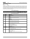
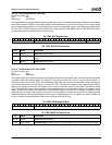
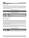
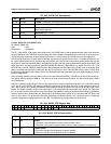
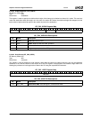
GP_BLT_MODE Register Map
31 30 29 28 27 26 25 24 23 22 21 20 19 18 17 16 15 14 13 12 11 10 9 8 7 6 5 4 3 2 1 0
RSVD
CP
TH X Y SM RSVD DR SR
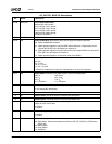
GP_BLT_MODE Bit Descriptions
Bit Name Description
31:12 RSVD Reserved. Write to 0.
11 CP Checkpoint. Generates interrupt when this BLT is completed if checkpoint interrupt is
enabled.
10 TH Throttle. BLT does not begin until next VBLANK.
0: Disable.
1: Enable.
9X X Direction.
0: Indicates a positive increment for the X position.
1: Indicates a negative increment for the X position.
8Y Y Direction.
0: Indicates a positive increment for the Y position.
1: Indicates a negative increment for the Y position.
7:6 SM Source Mode. Specifies the format of the source data.
00: Source is color bitmap.
01: Source is unpacked monochrome.
10: Source is byte-packed monochrome.
11: Undefined.
5:3 RSVD Reserved. Write as read.
2DR Destination Required.
0: No destination data is required.
1: Indicates that destination data is needed from frame buffer.
1:0 SR Source Required.
00: No source data.
01: Source from frame buffer.
10: Source from GP_HST_SRC register (GP Memory Offset 48h).
11: Undefined.


