AMD Geode™ LX Processors Data Book 229
GeodeLink™ Memory Controller Register Descriptions
33234H
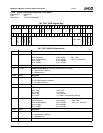
6.2.2.10 Timing and Mode Program (MC_CF8F_DATA)
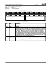
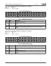
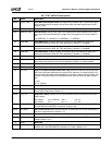
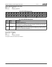
2 RSVD Reserved.
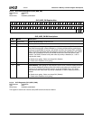
1SOFT_RST Software Reset. Puts the GLMC in a known state. Does not change configuration regis-
ters. The recommended sequence to use is:
1) Make sure SDRAM interface has “been idle for a while”.
2) Set software reset, then clear software reset.
3) Do a refresh cycle.
Accesses to memory may resume as normal following this.
Note that configuration registers are not scannable. To reproduce a problem in simulation
requires saving the configuration registers with software in silicon and reprogramming the
values in simulation. (Default = 0)
0PROG_DRAMProgram Mode Register in SDRAM. When this bit is set, the GLMC will issue one Load
Mode Register command to the DRAMs. It either programs the Mode Register (if
MSR_BA, bits [29:28] = 00), or the Extended Mode Register (if MSR_BA, bits [29:28] =
01). The Mode Register is programmed with CAS latency (see MSR 2000019h[30:28]),
wrap type sequential, and burst length of 4 for 64-bit data path, or burst length of 8 for 32-
bit wide data path. The Extended Mode Register in DDR DIMMs is programmed with the
QFC#, drive strength and DLL disable bits [26:24]. The Extended Mode Register must be
programmed first to enable the DLLs, then the Mode Register. This bit must be set and
cleared for each Load Mode Register command. (Default = 0)
MSR Address 20000019h
Typ e R /W
Reset Value 18000008_287337A3h
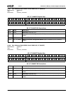
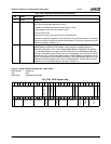
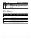
MC_CF07_DATA Bit Descriptions (Continued)
Bit Name Description
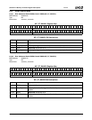
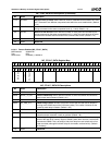
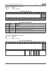
MC_CF8F_DATA Register Map
63 62 61 60 59 58 57 56 55 54 53 52 51 50 49 48 47 46 45 44 43 42 41 40 39 38 37 36 35 34 33 32
STALE_REQ RSVD
XOR_BIT_SEL
XOR_MB0
XOR_BA1
XOR_BA0
RSVD
TRUNC_DIS
REORDER_DIS
RSVD
HOI_LOI
RSVD
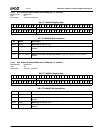
31 30 29 28 27 26 25 24 23 22 21 20 19 18 17 16 15 14 13 12 11 10 9 8 7 6 5 4 3 2 1 0
THZ_DLY
CAS_LAT ACT2ACTREF ACT2PRE
RSVD
PRE2ACT
RSVD
ACT2CMD ACT2ACT
DPLWR
DPLRD
RSVD


