354 AMD Geode™ LX Processors Data Book
Display Controller Register Descriptions
33234H
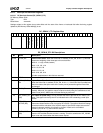
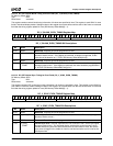
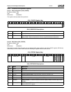
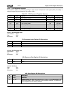
6.6.15.2 DC CRT Vertical Blank Timing for Even Fields (DC_V_BLANK_EVEN_TIMING)
This register contains vertical blank timing information. All values are specified in lines. This register is used ONLY for even
fields in interlaced display modes. Settings written to this register do not take effect until the start of the frame or interlaced
field after the timing register update bit is set (DC Memory Offset 008h[6] = 1).
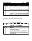
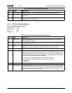
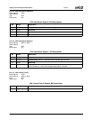
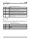
6.6.15.3 DC CRT Vertical Sync Timing for Even Fields (DC_V_SYNC_EVEN_TIMING)
This register contains CRT vertical sync timing information. All values are specified in lines. This register is used ONLY for
even fields in interlaced modes. Settings written to this register do not take effect until the start of the frame or interlaced
field after the timing register update bit is set (DC Memory Offset 008h[6] = 1).
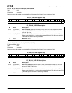
DC Memory Offset 0E8h
Typ e R /W
Reset Value xxxxxxxxh
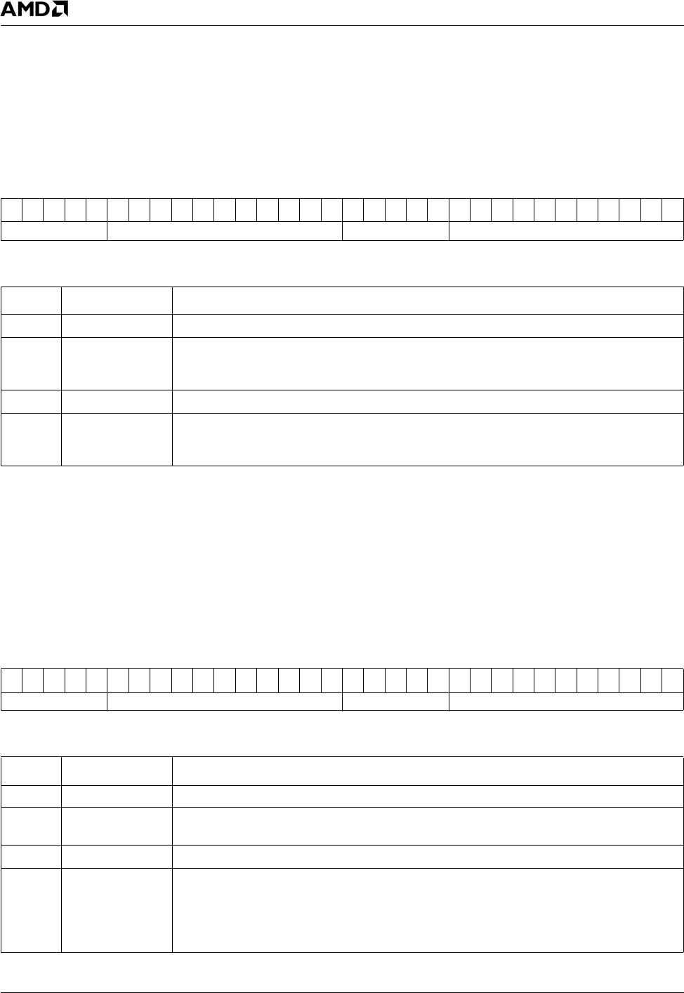
DC_V_BLANK_EVEN_TIMING Register Map
313029282726252423222120191817161514131211109876543210
RSVD V_BLANK_END RSVD V_BLANK_START
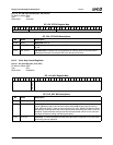
DC_V_BLANK_EVEN_TIMING Bit Descriptions
Bit Name Description
31:27 RSVD Reserved. These bits should be programmed to zero.
26:16 V_BLANK_END Vertical Blank End. This field represents the line at which the vertical blanking signal
becomes inactive minus 1. If the display is interlaced, no border is supported, so this
value should be identical to V_TOTAL (DC Memory Offset 0E4h[26:16]).
15:11 RSVD Reserved. These bits should be programmed to zero.
10:0 V_BLANK_
START
Vertical Blank Start. This field represents the line at which the vertical blanking signal
becomes active minus 1. If the display is interlaced, this value should be programmed to
V_ACTIVE (DC Memory Offset 0E4h[10:0]) plus 1.
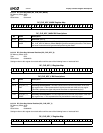
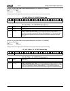
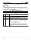
DC Memory Offset 0ECh
Typ e R /W
Reset Value xxxxxxxxh
DC_V_SYNC_EVEN_TIMING Register Map
313029282726252423222120191817161514131211109876543210
RSVD V_SYNC_END RSVD V_SYNC_START
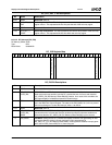
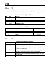
DC_V_SYNC_EVEN_TIMING Bit Descriptions
Bit Name Description
31:27 RSVD Reserved. These bits should be programmed to zero.
26:16 V_SYNC_END Vertical Sync End. This field represents the line at which the CRT vertical sync signal
becomes inactive minus 1.
15:11 RSVD Reserved. These bits should be programmed to zero.
10:0 V_SYNC_
START
Vertical Sync Start. This field represents the line at which the CRT vertical sync signal
becomes active minus 1. For interlaced display, note that the vertical counter is incre-
mented twice during each line and since there are an odd number of lines, the vertical
sync pulse will trigger in the middle of a line for one field and at the end of a line for the
subsequent field.


