


372 AMD Geode™ LX Processors Data Book
Display Controller Register Descriptions
33234H
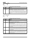
6.6.19.27 Line Compare
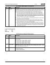
6.6.19.28 CPU Data Latch State
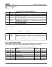
6.6.19.29 Attribute Index/Data FF State
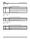
Index 18h
Typ e R /W
Reset Value 00h
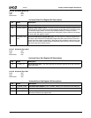
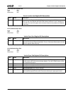
Line Compare Register Bit Descriptions
Bit Name Description
7:0 LINE_COMP[7:0] Line Compare Register Bits [7:0]. This value specifies the low eight bits of a compare
value that represents the scan line where the CRTC frame buffer address counter is
reset to 0. This can be used to create a split screen by using the Start Address registers
to specify a non-zero location at which to begin the screen image. The lower portion of
the screen (starting at frame buffer address 0) is immune to screen scrolling (and pel
panning as specified in the Attribute Mode Control register (Index 10h). Line Compare is
a 10-bit value. Bit 8 is located in the Overflow register (Index 07h[4]) and bit 9 is in the
Maximum Scan Line register (Index 09h[6]).
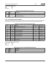
Index 22h
Typ e RO
Reset Value 00h
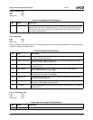
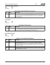
CPU Data Latch State Register Bit Descriptions
Bit Name Description
7:0 DLV Data Latch Value. This read only field returns a byte of the CPU data latches and can be
used in VGA save/restore operations. The graphics controller’s Read Map Select field
(Index 04h[1:0]) specifies which byte/map (0-3) is returned.
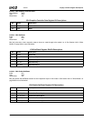
Index 24h
Typ e RO
Reset Value 00h
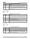
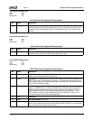
Attribute Index/Data FF State Register Bit Descriptions
Bit Name Description
7FFST FF State. This read only bit indicates the state of the attribute controller index/data flip-
flop. When this bit is 0, the next write to Index 3C0h will write an index value; when this
bit is 1, the next write to Index 3C0h will write a data register value.
6:0 RSVD Reserved.