


CHAPTER 3 SYSTEM CONTROLLER
204
Preliminary User’s Manual S15543EJ1V0UM
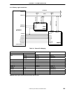
3.4 Memory Interface
The V
R
4120A accesses memory attached to the controller in the normal way, by addressing the memory space.
3.4.1 Overview
• 66 MHz or 100 MHz memory bus
• Supports up to 32 MB base memory range for SDRAM
• Supports up to 8 MB write-protectable boot memory range for PROM/flash
• On-chip programmable SDRAM refresh controller
• 4 words (16 bytes) prefetch data buffer (memory-to-V
R
4120A)
• PROM/flash data signals multiplexed on SDRAM data signals
• Programmable memory bus arbitration priority
• Programmable address ranges for the memory
• Programmable RAS-CAS delay (2, 3, 4 clocks)
• Programmable CAS latency (2, 3 clocks)
• Endian converter on IBUS slave I/F
• Don’t supports 8-word burst R/W from SysAD bus
3.4.2 Memory regions
The controller connects to memory directly and manages the addresses, data and control signals for the following
address ranges:
• One boot PROM/flash range (programmable)
• One system memory range (programmable)
The following types of memory modules as an example but not limited to, can be used:
• Flash with variable data size (8, 16, 32 bits) can be used in the boot ROM.
• PROM with variable data size (8, 16, 32 bits) can be used in the boot ROM.
• SDRAM can be used in the system memory.
Boot ROM can be populated with PROM or 85-ns flash chips. Prior to accessing PROM/flash, software must
configure this address range. The system memory can be populated with SDRAM chips. The system memory is used
for the RTOS, M/W and F/W. Prior to accessing SDRAM, software must configure this address range.