


CHAPTER 3 SYSTEM CONTROLLER
Preliminary User’s Manual S15543EJ1V0UM
217
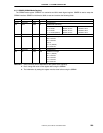
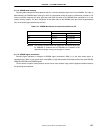
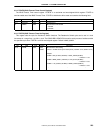
3.4.1.4 SDRAM word ordering
Following table indicates the word-address order for a 4-word instruction-cache line fill from SDRAM. This order is
determined by the SDRAM chips’ burst type, which is programmed during the memory initialization procedure. The
memory controller programs the burst type and word order the same for all SDRAM chips connected to it (in the
system memory ranges). The term “sequential” in this table refers to the SDRAM burst type. Burst length depends
only on the access type performed by the CPU.
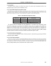
Table 3-10. SDRAM Word Order for Instruction-Cache Line-Fill
SDRAM-Chip Burst TypeStart Column Address A1.A0
Sequential Interleaved
00 0-1-2-3 Not supported
01 1-2-3-0 Not supported
10 2-3-0-1 Not supported
11 3-0-1-2 Not supported
Remark The memory controller does not support the interleaved burst type
for SDRAMs. It assumes that all SDRAMs are initialized to the
sequential burst type, using a burst length of 4 words.
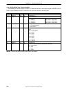
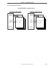
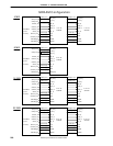
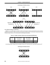
3.4.1.5 SDRAM signal connections
Following figure indicates an example of SDRAM signal connections. SMA [11] is the bank select signal. In
command cycle, SMA [11] low selects bank A and SMA [11] high selects bank B. Both banks share the same SDCSB,
SDRASB, SDCASB, and SDWEB signals.
The two banks of system memory behave as two halves of the address range, with the highest unmasked address
bit controlling bank selection.