


CHAPTER 2 V
R
4120A
92
Preliminary User’s Manual S15543EJ1V0UM
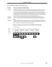
2.3.4.5 Load word instruction (LW rt, offset (base))
IF stage Same as the IF stage for the ADD instruction.
IT stage Same as the IT stage for the ADD instruction.
RF stage Same as the RF stage for the ADD instruction. Note that the base field is in the same position
as the rs field.
EX stage Refer to the EX stage for the ADD instruction. For LW, the inputs to the ALU come from
GPR[base] through the bypass multiplexer and from the sign-extended offset field. The result
of the ALU operation that is latched into the ALU output latch in
Φ
1 represents the effective
virtual address of the operand (DVA).
DC stage The cache tag field is compared with the Page Frame Number (PFN) field of the TLB entry.
After passing through the load aligner, aligned data is placed in the DC output latch during
Φ
2.
WB stage During
Φ
1, the cache read data is written into the register file addressed by the rt field.
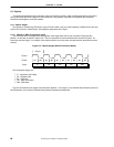
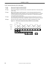
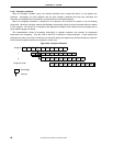
Figure 2-17. LW Instruction Pipeline Activities (In MIPS III Instruction Mode)
IF1
Cycle
Phase
PCycle
PClock
IF2
Φ
2
Φ
1
Φ
2
Φ
1
Φ
2
Φ
1
Φ
2
Φ
1
Φ
2
Φ
1
RF1 RF2 EX1 EX2 DC1 DC2 WB1 WB2
ITLB
IDC
ITC
ICA
IDEC
WBDVA
EXRF DCA
DL
DTLB
DT