


CHAPTER 7 PCI CONTROLLER
386
Preliminary User’s Manual S15543EJ1V0UM
7.4 Functions in Host-mode
The functions described in this section are available when PMODE is set to low.
7.4.1 Generating configuration cycle
7.4.1.1 How to generate Configuration Cycle
The PCI Controller can generates Configuration Cycle on PCI bus by accessing of the following two registers;
PCI Configuration Address Register (P_PCAR)
PCI Configuration Data Register (P_PCDR)
At first, the information like address to be accessed for Configuration Cycle has to be set to P_PCAR register.
Then, access to P_PCDR register generates Configuration Cycle on PCI bus.
7.4.1.2 PCI Configuration Address Register (P_PCAR)
Setting a ‘1’ to bit 31(Configuration Cycle Enable bit) enables generating Configuration Cycle. When this bit is set
to a ‘0’, access to P_PCDR register does not generate Configuration Cycle. The data will be ignored when a write
transaction is issued, and all “0” data will be returned when a read transaction is issued.
There are two types of Configuration Cycle, Type0 for PCI devices except for PCI bridges and Type1 for PCI
bridges, in PCI specification. The PCI Controller can generate both types of Configuration Cycle.
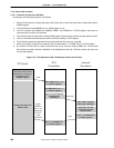
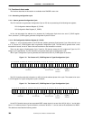
When Type1 Configuration Cycle is generated, the content to be set to P_PCAR register is as below;
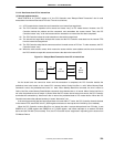
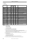
Figure 7-12. The Content of P_PCAR Register for Type0 Configuration Cycle
En
31 30
29
28 27
26
25
24 23 22 21 20 19 18 17
16
15 14
13 12 11
10
9
0
8765
4
3
0
21
0
Reserved
Device Number Function
Number
Register
Address
The PCI Controller sends this information on AD [31:0] at the address phase of the cycle. The content to be set to
P_PCAR register for Type 0 configuration cycle is as below;
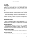
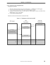
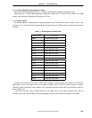
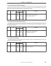
Figure 7-13. The Content of P_PCAR Register for Type1 Configuration Cycle
En
31 30
29
28 27
26
25
24 23 22 21 20 19 18 17
16
15 14
13 12 11
10
9
0
8765
4
3
1
21
0
Reserved Bus Number Device Number Function
Number
Register
Address
As the PCI Controller does not have separated IDSEL output signals, it set one bit of AD [31:16] to ‘1’ and all other
bits to ‘0’ in address phase of Type0 transaction, so that the bit set to ‘1’ can be used as the substitution for IDSEL.
The details are described the following section.