


CHAPTER 7 PCI CONTROLLER
406
Preliminary User’s Manual S15543EJ1V0UM
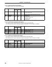
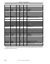
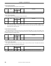
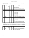
7.5.19.6 Revision ID register
This register specifies a device specific revision identifier.
R/WBits Field
Internal
bus
PCI
Default Description
7:0 Revision ID R R 01H Hardwired to ‘01H’ that shows the revision number of the chip.
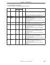
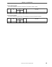
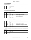
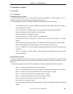
7.5.19.7 Class code register
This register is used to identify the generic function of the device.
R/WBits Field
Internal
bus
PCI
Default Description
23:0 Class Code R R 000302H
Note
Hardwired to ‘000302H’ that shows the class code of the chip.
Note When class code register in the configuration space is read, the wrong value “000302H” (related VGA) is
returned although “020300H” (ATM controller) should be returned as the class code of the
µ
PD98502. Please
change code on the Host driver side.
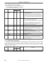
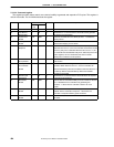
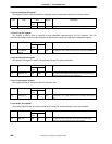
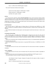
7.5.19.8 Cache line size register
This register specifies the system cache-line size in units of words (32-bit length). The value in this register is also
used to determine whether to use Memory Read, Memory Read Line, Memory Read Multiple, Memory Write and
Invalidate commands for accessing memory.
R/WBits Field
Internal
bus
PCI
Default Description
7:0 Cache Line
Size
R/W R/W 0 The system cache-line size in units of words.
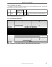
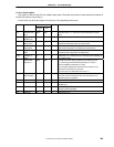
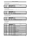
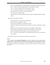
7.5.19.9 Latency timer register
This register specifies the value of the Latency Timer in units of PCI bus clocks. The bottom three bits are
hardwired to “0”s, so that a timer granularity is eight-clocks.
R/WBits Field
Internal
bus
PCI
Default Description
7:0 Latency Timer R/W R/W 0 The value of the Latency Timer in units of PCI bus clocks.