216 AMD Geode™ LX Processors Data Book
GeodeLink™ Memory Controller
33234H
6.1.1.3 Data Path
The write datapath utilizes three write buffers to gather
write data within a burst, each one is 4 deep x 64 bits.
Writes to the buffers are alternated between the three buff-
ers or whichever one is empty. The SID, PID, and implied
BEX are also buffered along with the write data. Once the
write request has been processed and arbitrated, and the
corresponding GLIU0 write data transfer is complete into
the buffers, the buffers are then read out and the write
command is dispatched out to memory. Which of the three
buffers is read out depends on which buffer’s SID, PID
matches the SID, PID of the write request that won the
arbitration for the DRAM. If more than one buffer’s SID,
PID matches the write request’s SID, PID, then the buffer
with the older data is read out. The write data is clocked out
using a delay-tuned version of the GLMC/SDRAM write
clock. Only one transaction’s set of write data is written into
a buffer; therefore, only three write transactions can be
buffered at any time.
The write data is written into and read out of the buffers on
the GLIU0 clock, which is twice the frequency of the
GLMC/SDRAM clock. The data strobes DQS are also
shipped out with each data beat, center-aligned with the
data to strobe the data into the DRAM. Unlike SDRAM,
there is a write latency tDQSS between the write command
and the first write data presented to DRAM.
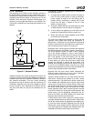
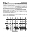
Read data is not buffered to minimize latency. The DQS
strobes generated by the DRAM are edge-aligned with the
read data, and are used to register the read data.The clock
ratio between the GLIU0 clock and GLMC clock is a syn-
chronous 2:1. Since the arrival of the data can vary by as
much as one clock from byte to byte, and vary over time
and temperature, the GLMC captures and resyncs the data
byte by byte as it becomes valid.
6.1.1.4 GLMC/GLCP/Pad Delay Control Settings
GLMC signals to and from the pads are controlled with var-
ious delay lines in the pads. These delay lines are pro-
grammable in the GLCP module. For details on these
delay controls, refer to the Section 6.14.2.8 "GLCP I/O
Delay Controls (GLCP_DELAY_CONTROLS)" on page
549.
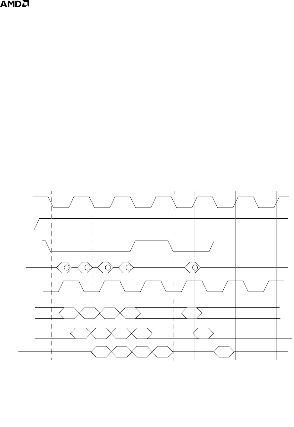
6.1.1.5 Basic Timing Diagrams
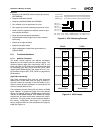
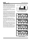
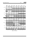
Figure 6-8 and Figure 6-9 on page 217 illustrate timing
waveforms for DDR reads and DDR writes.
Figure 6-8. DDR Reads
rd3
rd1rd0 rd0
drdywx
m_sd_data
daout
drdyrx
clock
ds
r_data_sync
rd2
rd3
rd1rd0 rd0rd2
r_data_pad
rd3
rd1rd0 rd0rd2


