340 AMD Geode™ LX Processors Data Book
Display Controller Register Descriptions
33234H
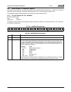
6.6.9.3 DC Dirty/Valid RAM Access (DC_DV_ACCESS)
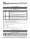
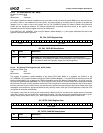
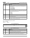
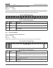
11:10 DV_LINE_SIZE DV Line Size. This field determines how many bytes of frame buffer space correspond
to an entry in the DV RAM. The value selected by this field must be greater than or
equal to the FB_LINE_SIZE, as programmed in the DC_LINE_SIZE register (DC Mem-
ory Offset 030h[9:0]).
00: 1024 (256 QWORDs)
01: 2048 (512 QWORDs)
10: 4096 (1024 QWORDs)
11: 8192 (2048 QWORDs)
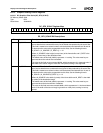
9:8 DV_RANGE DV Range. The value selected by this field is an upper bound of the number of entries
used in the DV RAM. By setting this value to a number less than the maximum (2048),
there is a potential savings in power, since the DV RAM will not be accessed for lines
that may be just above the frame buffer space.
00: 2048 lines
01: 512 lines
10: 1024 lines
11: 1536 lines
7:2 RSVD Reserved. Set to 0.
1 DV_MASK DV MASK. While this bit is set, the DV RAM controller does not monitor writes to mem-
ory; no DIRTY bits will be set in response to memory activity. When this bit is cleared,
the DV RAM behaves normally.
0 CLEAR_DV_RAM Clear DV RAM. Writing a 1 to this bit causes the contents of the DV RAM to be cleared
(i.e., every entry is set to dirty and invalid). This process requires approximately 2050
GLIU0 clocks. This bit may be read to determine if this clear operation is underway (1)
or completed (0). Writing a 0 to this bit has no effect.
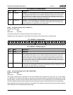
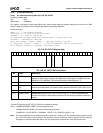
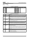
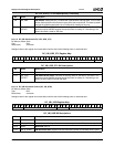
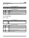
DC Memory Offset 08Ch
Typ e R /W
Reset Value 0000000xh
DV_CTL Bit Descriptions (Continued)
Bit Name Description
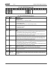
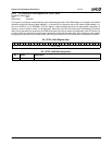
DC_DV_ACCESS Register Map
313029282726252423222120191817161514131211109876543210
RSVD
DV_VALID
DV_DIRTY
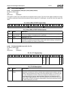
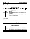
DC_DV_ACCESS Bit Descriptions
Bit Name Description
31:2 RSVD Reserved. Set to 0.
1DV_VALID DV Valid. Writes to this register place the value of this bit into the “valid” entry of the DV
RAM. Reads return the value of the “valid” entry. The DV RAM Address is determined by
the value in DV_RAM_AD (DC Memory Offset 084h[10:0]).
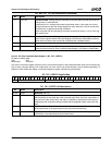
0DV_DIRTY DV Dirty. Writes to this register will place the value of this bit into the “dirty” entry of the
dirty/valid RAM. Reads will return the value of the “dirty” entry. The DV RAM Address is
determined by the value in DV_RAM_AD (DC Memory Offset 084h[10:0]).


