410 AMD Geode™ LX Processors Data Book
Video Processor
33234H
CRC Signature
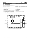
The FP contains hardware/logic that performs Cyclical
Redundancy Checks (CRCs) on the panel data digital pipe-
line. This feature is used for error detection and makes it
possible to capture a unique 24- or 32-bit signature for any
given mode setup. An error in the dither pixel pipeline pro-
duces a different signature when compared to a known
good signature value. The dither data path can be config-
ured in two basic modes: dither enable and dither disable
by programming the DENB bit (FP Memory Offset 418h[0]).
This allows the programmer to quickly and accurately test a
video screen without having to visually inspect the screen
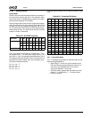
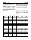
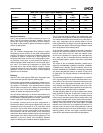
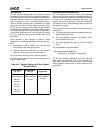
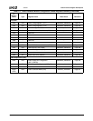
for errors. Table 6-67 shows the bit settings that provide
this feature.
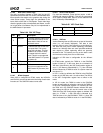
Panel selection is done through FP Memory Offset
408h[18:16]. The selection of these bits results in two func-
tions.
1) Generates the desired PANEL CLK from the pixel
clock based on the panel type selected.
2) Steers the internal pixel bus on to the panel interface
data pins. All the unused pins are driven with 0s.
This panel data is sent to the CRC signature generator.
The CRC number varies for each panel configuration for a
fixed on-screen image.
Addressing the Dithering Memories
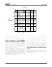
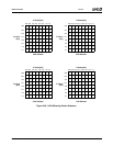
The least significant four bits of each color component
intensity value are used to select a 4x4 dithering pattern. In
other words, there are 16 different 16-bit dithering patterns
for each color component (red, green, and blue). This
requires one 256x1-bit memory for each color component.
The address to one of these dithering pattern memories is
then eight bits in length.
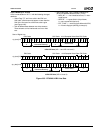
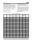
The bit address for dithering memory is defined as the con-
catenation of:
1) The least significant two bits of the display screen hori-
zontal position pixel count
2) The least significant two bits of the display screen
vertical position pixel count
3) The least significant four bits of the input intensity
value
This concatenation is as shown below:
The FP GLIU interface programs the red, green, and blue
dither memories individually, or all at once. Writing to all
three dither memories at the same time means that the
dithering patterns are the same for each of the three color
components.
Table 6-67. Register Settings for Dither Enable/
Disable Feature
Dither Enable
for TFT
Bypass Dither
for TFT Bypass FP
FP Memory
Offset 418h[6:0]
000,001,1
001,010,1
010,011,1
011,100,1
100,101,1
101,xxx,x
FP Memory
Offset 418h[6:0]
101,xxx,x
FP Memory
Offset 408h[30]
is set to 1
Dithering Memory Bit Address[7:0]
= {X-Count[1:0], Y-Count[1:0], Intensity[3:0]}


