552 AMD Geode™ LX Processors Data Book
GeodeLink™ Control Processor Register Descriptions
33234H
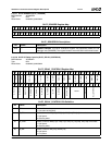
6.14.2.10 GLCP Clock Active (GLCP_CLKACTIVE)
See "GLCP_CLKOFF Bit Descriptions" on page 551 for bit descriptions.
11 DCDOT_0 DC Dot Clock Off. When set, disables DC Dot Clock 0 (DC).
10 GLIU0_1 GLIU0Clock Off. When set, disables main clock to primary GLIU.
9GLIU0_0 GLIU0 Timer Logic Clock Off. When set, disables clock to timer logic of primary
GLIU.
8GP GP Clock Off. When set, disables GP clock (GLIU).
7GLMC GLMC Clock Off. When set, disables GLIU clock to memory controller.
6 DRAM DRAM Clocks Off. When set, disables external DRAM clocks (and, hence, feedback
clocks).
5 BC_GLIU Bus Controller Clock Off. When set, disables clock to CPU bus controller block.
4BC_VA CPU to Bus Controller Clock Off. When set, disables CPU clock to bus controller
block.
3MSS CPU to MSS Clock Off. When set, disables CPU clock to MSS block.
2 IPIPE CPU to IPIPE Clock Off. When set, disable CPU clock to IPIPE block.
1 FPUFAST FPU Fast Clock Off. When set, disables the fast FPU clock.
0 FPUSLOW FPU Clock Off. When set, disables the slow CPU clock to FPU.
MSR Address 4C000011h
Typ e RO
Reset Value Input Determined
GLCP_CLKOFF Bit Descriptions (Continued)
Bit Name Description
GLCP_CLKACTIVE Register Map
63 62 61 60 59 58 57 56 55 54 53 52 51 50 49 48 47 46 45 44 43 42 41 40 39 38 37 36 35 34 33 32
RSVD
VIPVIP
VIPGLIU
313029282726252423222120191817161514131211109876543210
AES
AESGLIU
AESEE
GLCPDBG
GLCPGLIU
GLCPPCI
VPVOP
VPDOT_2
VPDOT_1
VPDOT_0
VPGLIU_1
VPGLIU_0
PCIPCIF
PCIPCI
PCIGLIU
GLIU1_1
GLIU1_0
DCGLIU_1
DCGLIU_0
RSVD
DCDOT_0
GLIU0_1
GLIU0_0
GP
GLMC
DRAM
BC_GLIU
BC_VA
MSS
IPIPE
FPUFAST
FPUSLOW


