AMD Geode™ LX Processors Data Book 377
Display Controller Register Descriptions
33234H
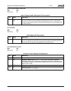
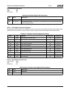
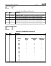
6.6.20.9 VGA Miscellaneous
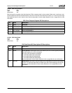
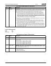
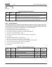
1:0 WR_MD Write Mode. This field specifies how CPU data is written to the frame buffer. Note that
the Write Operation field in the VGA Data Rotate register (Index 03h[4:3]) specifies how
CPU data is combined with data in the data latches for write modes 0, 2, and 3.
00: Write Mode 0: CPU data is rotated by the count in the VGA Data Rotate register.
Each map enabled by the VGA Map Mask Register (Index 02h) is written by the
rotated CPU data combined with the latch data (if set/reset is NOT enabled for that
map) or by the map’s corresponding set/reset bit replicated across the 8-bit byte (if
set/reset IS enabled for that map). The VGA Bit Mask Register (Index 08h) is used to
protect individual bits in each map from being updated.
01: Write Mode 1: Each map enabled by the VGA Map Mask Register is written with its
corresponding byte in the data latches.
10: Write Mode 2: CPU data is replicated for each map and combined with the data
latches and written to memory. The VGA Bit Mask Register (Index 08h) is used to
protect individual bits in each map from being updated.
11: Write Mode 3: Each map is written with its corresponding Set/Reset bit replicated
through a byte (Enable Set/Reset is ignored). The CPU data is rotated and ANDed
with the VGA Bit Mask Register (Index 08h). The resulting mask is used to protect
individual bits in each map.
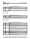
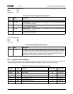
Index 06h
Typ e R /W
Reset Value xxh
VGA Miscellaneous Register Bit Descriptions
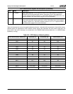
Bit Name Description
7:4 RSVD Reserved.
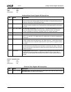
3:2 MEM_MAP Memory Map. This field controls the address mapping of the frame buffer in the CPU
memory space.
00: Memory Map 0: A0000 to BFFFF (128 KB)
01: Memory Map 1: A0000 to AFFFF (64 KB)
10: Memory Map 2: B0000 to B7FFF (32 KB)
11: Memory Map 3: B8000 to BFFFF (32 KB)
1 ODD_EVEN Odd/Even. When set to 1, this bit replaces the CPU A0 address bit with a higher order bit
when addressing the frame buffer. Odd maps are then selected when CPU A0 = 1, and
even maps selected when CPU A0 = 0.
0GPH_MD Graphics Mode.
0: Text mode operation.
1: Graphics mode operation.
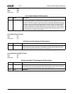
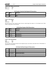
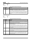
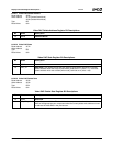
VGA Graphics Mode Register Bit Descriptions
Bit Name Description


