534 AMD Geode™ LX Processors Data Book
GeodeLink™ Control Processor
33234H
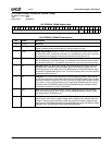
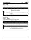
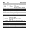
Table 6-81. TAP Control Instructions (25-Bit IR)
Instruction
DR
Length IR Name Description
123FFFAh 8 BYPASS_MODES This register is read/write.
127FFFAh 8 REVID Should be 10h for initial AMD Geode™ LX processor (upper
nibble is major rev, lower nibble is minor) changes for each
metal spin
1FFFEB0h 441 MULTISCAN Parallel scan (muxes scan outputs onto many chip pins)
1FFFFDFh 1 TRISTATE Put chip into TRI-STATE and comparison mode
1FFFFFDh 29 BISTDR Parallel RAM BIST - internal data register (for chip test)
1FFFFFEh 32 IDCODE ID Code = 0D5A1003h
1FFFFFFh 1 BYPASS Bypass; IEEE 1149.1 spec requires all 1s to be bypass
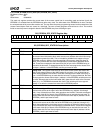
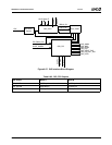
Table 6-82. TAP Instruction Bits
Bit Name Description
24 TAPSCAN# Also USER[6] in the design. This is a user bit added by AMD; low indicates that an inter-
nal scan chain is accessed by the TAP.
23:18 USER[5:0] User bits used to identify an internal scan chain or, if bit 24 is high, to access a special
internal DR, as shown in Table 6-81.
17:16 bistEnable[4:3] Bits 4 and 3 of the BIST enable for individual BIST chain access.
15:13 clkRatio[2:0]# Not used in the AMD Geode™ LX processor (bits should always be high); clock ratio
controls for LogicBist.
12 freezeMode Not used in the AMD Geode LX processor (should always be high); another clock con-
trol signal.
11:10 setupMode[1:0]# Not used in the AMD Geode LX processor (should always be high); these are special
BIST controller bits.
9:7 bistEnable[2:0] BIST[2:0] of BIST enable. Works in conjunction with bits [17:16].
6 testMode# Active low TEST_MODE for entire chip. Puts internal logic into scan test mode.
5 forceDis# Active low bit TRI-STATEs all output pins.
4 selectJtagOut# Active low bit that allows boundary scan cells to control pads.
3 selectJtagIn# Active low bit that allows boundary scan cells to drive data into core logic of chip.
2:0 OP[2:0] Opcode that selects how the JTAG chains are wired together.


