376 AMD Geode™ LX Processors Data Book
Display Controller Register Descriptions
33234H
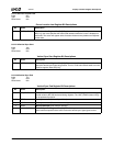
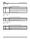
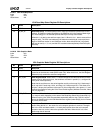
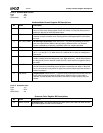
6.6.20.7 VGA Read Map Select
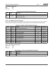
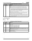
6.6.20.8 VGA Graphics Mode
Index 04h
Typ e R /W
Reset Value xxh
VGA Read Map Select Register Bit Descriptions
Bit Name Description
7:2 RSVD Reserved.
1:0 R_MP_SL Read Map Select. This field specifies which map CPU read data is taken from in read
mode 0. In Odd/Even modes (specified by the Odd/Even bit in the Graphics Mode regis-
ter, Index 05h[4]) bit 1 of this field specifies which pair of maps returns data.
When bit 1 is 0, data is returned from maps 0 and 1. When bit 1 is 1, data is returned from
maps 2 and 3. The CPU read address bit A0 determines which byte is returned (low or
high) in Odd/Even modes. In non-Odd/Even modes, these bits (both bits [1:0]) specify
the map to read (0, 1, 2, or 3) and the CPU accesses data sequentially within the speci-
fied map.
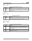
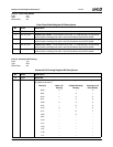
Index 05h
Typ e R /W
Reset Value xxh
VGA Graphics Mode Register Bit Descriptions
Bit Name Description
7 RSVD Reserved.
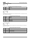
6 256_CM 256 Color Mode. When set to a 1, this bit configures the video serializers in the graphics
controller for the 256 color mode (BIOS mode 13h). When this bit is 0, the Shift Register
Mode bit (bit 5) controls the serializer configuration.
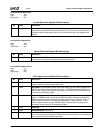
5 SH_R_MD Shift Register Mode. When set to a 1, this bit configures the video serializers for BIOS
modes 4 and 5. When this bit is 0, the serializers are taken in parallel (i.e., configured for
4-bit planar mode operation).
Note that the serializers are also wired together serially so that map 3 bit 7 feeds map 2
bit 0, map 2 bit 7 feeds map 1 bit 0, and map 1 bit 7 feeds map 0 bit 0. This allows for a
32-pixel 1 bit-per-pixel serializer to be used. For this configuration, color planes 1, 2, and
3 should be masked off using the Color Plane Enable register (Attribute Controller, Index
12h, on page 381.)
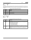
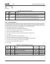
4 ODD_EVEN Odd/Even. When this bit is set to 1, CPU address bit A0 will select between maps 0 and
1 or maps 2 and 3 depending on the state of the Read Map Select field (Index 04h[1:0]).
When this bit is 0, the CPU accesses data sequentially within a map. This bit is equiva-
lent to the Odd/Even bit in the VGA Miscellaneous register (Index 06h[2]), but is inverted
in polarity from that bit.
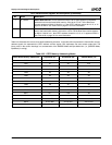
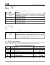
3 RD_MD Read Mode. This bit determines what is returned to the CPU when it reads the frame
buffer. When this bit is 1, the result of a color compare operation is returned. The eight
bits in the CPU read data contain a 1 in each pixel position where the color compare
operation was true, and a 0 where the operation was false. When this bit is 0, frame
buffer map data is returned.
2 RSVD Reserved.


