AMD Geode™ LX Processors Data Book 265
Graphics Processor Register Definitions
33234H
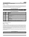
6.4.2.10 Pattern Data (GP_PAT_DATA_x)
In solid pattern mode, these registers are not used.
In monochrome pattern mode, GP_PAT_DATA_0 and GP_PAT_DATA_1 combine to hold the entire 8x8 pattern (64 bits).
GP_PAT_DATA_0[7:0] is the first line of the pattern, with bit 7 corresponding to the leftmost pixel on the screen.
GP_PAT_DATA_1[31:24] is the last line of the pattern.
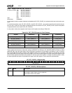
In color pattern mode, these registers each hold part of the pattern according to Table 6-31.
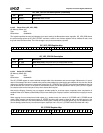
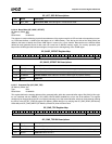
6.4.2.11 Raster Mode (GP_RASTER_MODE)
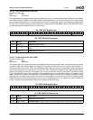
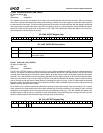
This register controls the manipulation of the pixel data through the graphics pipeline. Refer to section Section 6.3.10 "Ras-
ter Operations (ROP)" on page 251 for more information on the functionality of the ROP and Section 6.3.11 "Image Com-
positing Using Alpha" on page 252 for information on alpha blending and compositing. This register is byte writable to allow
modification of the ROP and other control bits without having to rewrite the BPP and FMT every time.
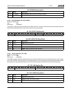
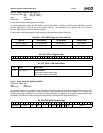
GP Memory Offset 30h GP_PAT_DATA_0
34h GP_PAT_DATA_1
Typ e R /W
Reset Value 00000000h
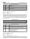
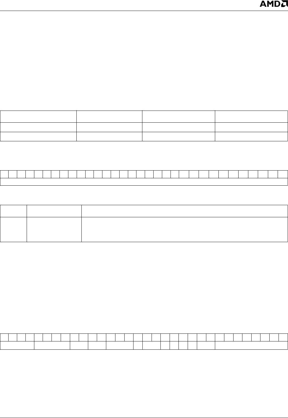
Table 6-31. PAT_DATA Usage for Color Patterns
Register 8-bpp Mode 16-bpp Mode 32-bpp Mode
GP_PAT_DATA_0 Line 0, pixels 3-0 Line 0, pixels 1-0 Line 0, pixel 0
GP_PAT_DATA_1 Line 0, pixels 7-4 Line 0, pixels 3-2 Line 0, pixel 1
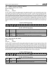
GP_PAT_DATA_x Register Map
31 30 29 28 27 26 25 24 23 22 21 20 19 18 17 16 15 14 13 12 11 10 9 8 7 6 5 4 3 2 1 0
PAT_DATA_ x
GP_PAT_DATA_x Bit Descriptions
Bit Name Description
31:0 PAT_DATA _x Pattern Data x.
Mono pattern mode: Pattern data.
Color pattern mode: Color pattern.
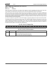
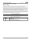
GP Memory Offset 38h
Typ e R /W
Reset Value 00000000h
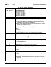
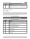
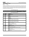
GP_RASTER_MODE Register Map
31 30 29 28 27 26 25 24 23 22 21 20 19 18 17 16 15 14 13 12 11 10 9 8 7 6 5 4 3 2 1 0
BPP/FMT RSVD EN OS AS
CS
RSVD SI PI ST PT PM ROP/a
R


