AMD Geode™ LX Processors Data Book 359
Display Controller Register Descriptions
33234H
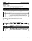
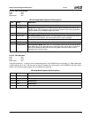
6.6.18.4 VGA Clocking Mode
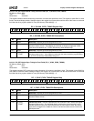
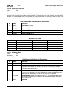
6.6.18.5 VGA Map Mask
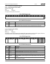
These bits enable (bit = 1) writing to their corresponding bytes in each DWORD of the frame buffer (i.e., EM3 enables byte
3, EM2 enables byte 2, etc.). The four maps or planes correspond to the four bytes in each DWORD of the frame buffer.
Reads to all maps are always enabled, and are unaffected by these bits.
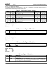
Index 01h
Typ e R /W
Reset Value 02h
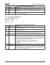
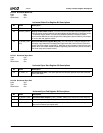
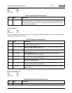
VGA Clocking Mode Register Bit Descriptions
Bit Name Description
7:6 RSVD Reserved.
5 SCREEN_OFF Screen Off. Setting this bit to a 1 blanks the screen while maintaining the HSYNC and
VSYNC signals. This is intended to allow the CPU full access to the memory bandwidth.
This bit must be 0 for the display image to be visible.
4 RSVD Not Supported. (Shift4)
3 DCLK_DIV2 Dot Clock Divide By 2. When set to 1, the incoming pixel clock is divided by two to form
the actual Dot clock. When 0, the incoming pixel clock is used unchanged.
2 RSVD Not Supported. (Shift Load)
1 RSVD Reserved. Always 1.
0 CHAR_WIDTH 8-Dot Character Width. When set to a 1, the character cells in text mode are eight pixels
wide. When set to 0, the character cells are nine pixels wide. The 9th pixel is equal to the
8th pixel for character codes C0h-DFh (the line graphics character codes), and is 0
(background) for all other codes.
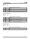
Index 02h
Typ e R /W
Reset Value 00h
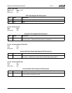
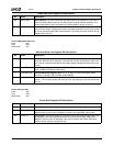
VGA Map Mask Register Bit Descriptions
Bit Name Description
7:4 RSVD Reserved.
3EM3 Enable Map 3.
2EM2 Enable Map 2.
1EM1 Enable Map 1.
0EM0 Enable Map 0.


