AMD Geode™ LX Processors Data Book 411
Video Processor
33234H
6.7.8 VP Resolution Table
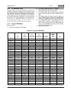
Supported CRT and flat panel resolutions of the VP are
provided in Table 6-32 on page 281. All resolutions can be
up to 8 bits per color, or 24 bits per pixel. In general, all dis-
play resolutions contained in VESA Monitor Timing Specifi-
cations Version 1.0 v0.8 are supported for CRT. Flat panels
up to 1600x1200x60 are supported. For those resolutions
not listed in the VESA specification, the maximum Dot
clock frequency is 340 MHz for CRT and 170 MHz for TFT.
All SDTV and HDTV resolutions are also supported
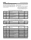
6.7.9 Display RGB Modes
Mode overview:
1) CRT: Normal functional, CRT display.
2) TFT Online: Normal functional, TFT display.
3) CRT Legacy RGB: Use companion device as off-chip
display controller, graphics only for CRT.
4) TFT Legacy RGB: Use the AMD Geode companion
device as off-chip display controller, graphics only for
CRT.
5) CRT Debug: Normal functional, access to debug sig-
nals. The DBG signals are driven on the specified pins
outside the VP module, listed here for information only.
6) TFT Legacy RGB Debug: Use companion device as
off-chip display controller, reduced graphics only for
CRT, access to debug signals. The DBG signals are
driven on the specified pins outside the VP module,
listed here for information only.
7) VOP: Normal function
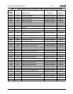
Table 6-68. Display RGB Modes
Pin
CRT
1
TFT
ONLINE
2
CRT
Legacy RGB
3
TFT
Legacy RGB
4
CRT Debug
5
TFT
LEGACY
RGB
Debug
6
VOP
7
DRGB23 0 TFT23 R7 R7 DBG15 DBG15 0
DRGB22 0 TFT22 R6 R6 DBG14 DBG14 0
DRGB21 0 TFT21 R5 R5 DBG13 DBG13 0
DRGB20 0 TFT20 R4 R4 DBG12 DBG12 0
DRGB19 0 TFT19 R3 R3 DBG11 DBG11 0
DRGB18 0 TFT18 0 R2 0 R7 0
DRGB17 0 TFT17 0 R1 0 R6 0
DRGB16 0 TFT16 0 R0 0 R5 0
DRGB15 0 TFT15 G7 G7 DBG10 DBG10 VOP8
DRGB14 0 TFT14 G6 G6 DBG09 DBG09 VOP9
DRGB13 0 TFT13 G5 G5 DBG08 DBG08 VOP10
DRGB12 0 TFT12 G4 G4 DBG07 DBG07 VOP11
DRGB11 0 TFT11 G3 G3 DBG06 DBG06 VOP12
DRGB10 0 TFT10 G2 G2 DBG05 DBG05 VOP13
DRGB9 0 TFT9 0 G1 0 G7 VOP14
DRGB8 0 TFT8 0 G0 0 G6 VOP15
DRGB7 0 TFT7 B7 B7 DBG04 DBG04 VOP0
DRGB6 0 TFT6 B6 B6 DBG03 DBG03 VOP1
DRGB5 0 TFT5 B5 B5 DBG02 DBG02 VOP2
DRGB4 0 TFT4 B4 B4 DBG01 DBG01 VOP3
DRGB3 0 TFT3 B3 B3 DBG00 DBG00 VOP4
DRGB2 0 TFT2 0 B2 0 G5 VOP5
DRGB1 0 TFT1 0 B1 0 B7 VOP6
DRGB0 0 TFT0 0 B0 0 B6 VOP7
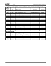
DOTCLK 0 FP_SHFCLK DF_DOT_CLK DF_DOT_CLK DBG_CLK DF_DOT_CLK VOPCLK
HSYNC VP_HSYNC FP_HSYNC VG_HSYNC VG_HSYNC VP_HSYNC VG_HSYNC 0
VSYNC VP_VSYNC FP_VSYNC VG_VSYNC VG_VSYNC VP_VSYNC VG_VSYNC 0
DISPEN 0 BKLEN 0 VG_DISP_EN 0 VG_DISP_EN 0
VDDEN 0 FP_VDDEN 0 0 0 0 0
LDEMOD 0 FP_LDE 0 0 0 0 0


