AMD Geode™ LX Processors Data Book 527
Security Block Register Descriptions
33234H
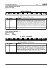
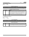
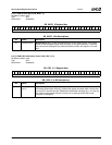
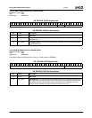
6.12.3.13 SB Writable Key 3 (SB_WKEY_3)
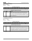
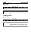
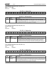
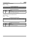
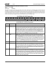
6.12.3.14 SB CBC Initialization Vector 0 (SB_CBC_IV_0)
SB Memory Offset 03Ch
Typ e WO
Reset Value 00000000h
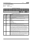
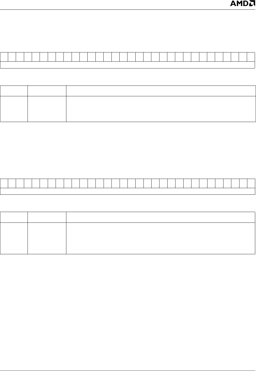
SB_WKEY_3 Register Map
313029282726252423222120191817161514131211109876543210
WKEY_3[127:96]
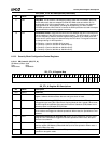
SB_WKEY_3 Bit Descriptions
Bit Name Description
31:0 Writable Key 3 Writable Key 3. Bits [127:96] of the Writable Key for the Security Block. This register
should not be changed during an AES encryption or decryption operation. To prevent
one process from reading the key written by another process, this register is not read-
able.
SB Memory Offset 040h
Typ e R /W
Reset Value 00000000h
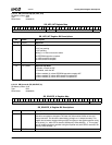
SB_CBC_IV_0 Register Map
31 30 29 28 27 26 25 24 23 22 21 20 19 18 17 16 15 14 13 12 11 10 9 8 7 6 5 4 3 2 1 0
CBC_IV_0[31:0]
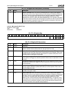
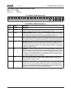
SB_CBC_IV_0 Bit Descriptions
Bit Name Description
31:0 CBC_IV_0
[31:0]
CBC Initialization Vector 0 [31:0]. Bits [31:0] of the initialization vector (IV) for the CBC
AES mode (Cipher Block Chaining). Change this register only when both A and B chan-
nels are IDLE. (A and B start bits, SB Memory Offset 000h and 004h, bit 0 = 0). This reg-
ister must be programmed with the IV vector prior to starting an AES CBC mode
encryption or decryption.


