


www.ti.com
7C64x+PeripheralInformationandElectricalSpecifications
7.1ParameterInformation
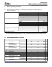
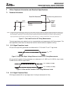
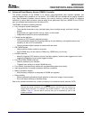
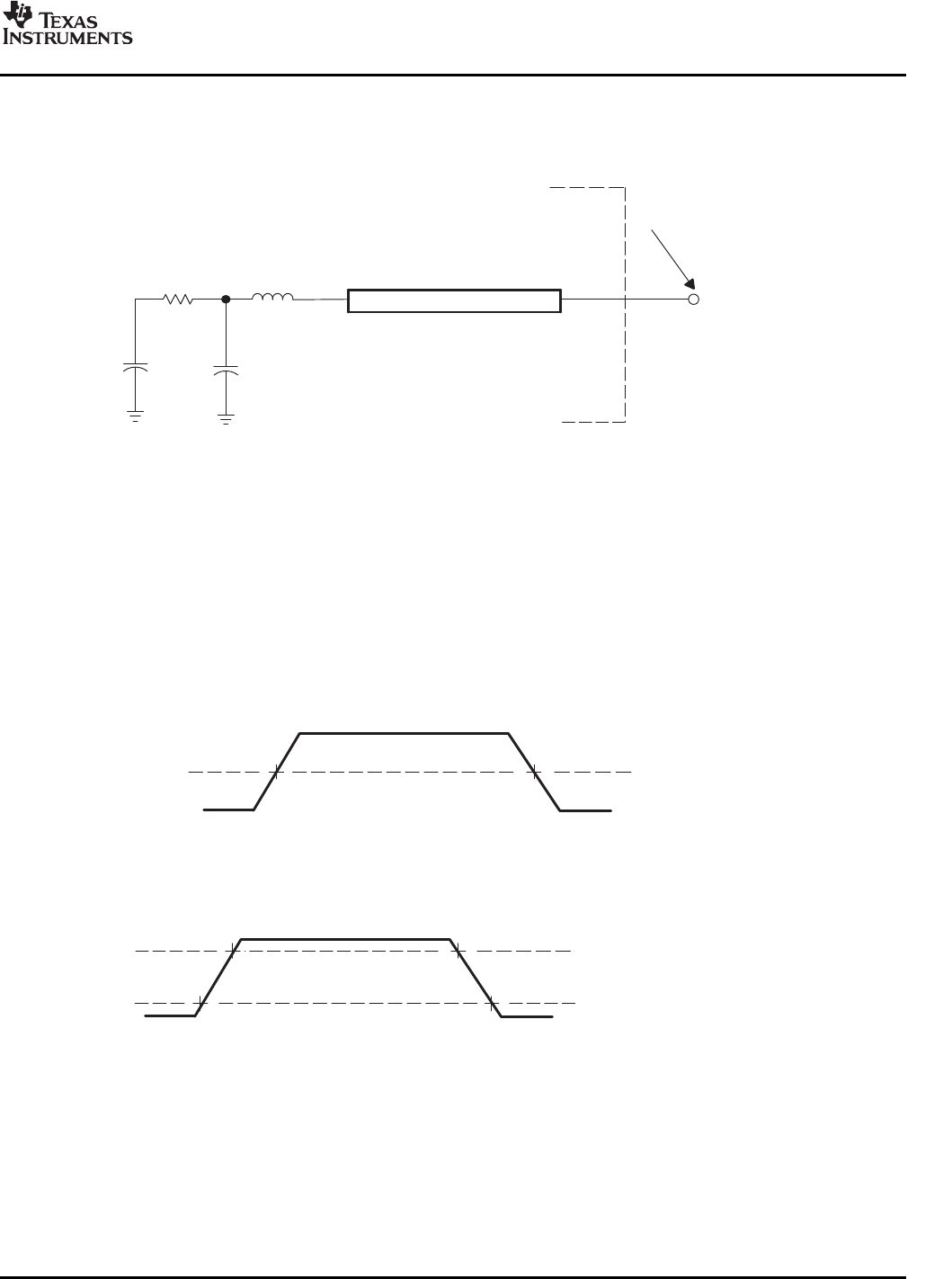
Transmission Line
4.0 pF 1.85 pF
Z0 = 50 Ω
(see Note)
Tester Pin Electronics
Data Sheet Timing Reference Point
Output
Under
Test
NOTE: This data sheet provides timing at the device pin. For output timing analysis, the tester pin electronics and its transmission line effects must
be taken into account. A transmission line with a delay of 2 ns can be used to produce the desired transmission line effect. The transmission
line is intended as a load only. It is not necessary to add or subtract the transmission line delay (2 ns) from the data sheet timings.
Input requirements in this data sheet are tested with an input slew rate of < 4 Volts per nanosecond (4 V/ns) at the device pin.
42 Ω 3.5 nH
Device Pin
(see Note)
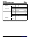
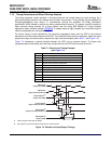
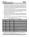
7.1.13.3-VSignalTransitionLevels
V
ref
= 1.5 V
V
ref
= V
IL
MAX (or V
OL
MAX)
V
ref
= V
IH
MIN (or V
OH
MIN)
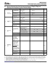
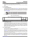
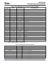
7.1.23.3-VSignalTransitionRates
SM320C6455-EP
FIXED-POINTDIGITALSIGNALPROCESSOR
SPRS462B–SEPTEMBER2007–REVISEDJANUARY2008
Figure7-1.TestLoadCircuitforACTimingMeasurements
TheloadcapacitancevaluestatedisonlyforcharacterizationandmeasurementofACtimingsignals.This
loadcapacitancevaluedoesnotindicatethemaximumloadthedeviceiscapableofdriving.
Allinputandoutputtimingparametersarereferencedto1.5Vforboth"0"and"1"logiclevels.
Figure7-2.InputandOutputVoltageReferenceLevelsforACTimingMeasurements
AllriseandfalltransitiontimingparametersarereferencedtoV
IL
MAXandV
IH
MINforinputclocks,
V
OL
MAXandV
OH
MINforoutputclocks.
Figure7-3.RiseandFallTransitionTimeVoltageReferenceLevels
Alltimingsaretestedwithaninputedgerateof4voltspernanosecond(4V/ns).
SubmitDocumentationFeedbackC64x+PeripheralInformationandElectricalSpecifications105