


www.ti.com
5C64x+Megamodule
A register file
Data path 1 Data path 2
B register file
D2 S2
xx
xx
M2
L2
Instruction decode
M1
xx
xx
L1 S1 D1
16/32−bit instruction dispatch
Instruction fetch
SPLOOP buffer
64 64
C64x+ CPU
256
32
L1D cache/SRAM
Bandwidth management
Memory protection
L1 data memory controller
IDMA
256
256
Bandwidth management
L1 program memory controller
Memory protection
256
Advanced event
triggering
(AET)
Interrupt
and exception
controller
Power control
L2 memory
controller
256
256
Master DMA
Slave DMA
128
256
L1P cache/SRAM
L2
cache/
SRAM
256
128
128
To primary
switch fabric
Cache
control
Bandwidth
management
Memory
protection
Cache control
Cache control
Internal
ROM
(A)
256
Configuration
Registers
32
To Chip
registers
External memory
controller
A. When accessing the internal ROM of the DSP, the CPU frequency must be less than 750 MHz.
5.1MemoryArchitecture
SM320C6455-EP
FIXED-POINTDIGITALSIGNALPROCESSOR
SPRS462B–SEPTEMBER2007–REVISEDJANUARY2008
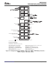
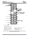
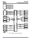
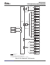
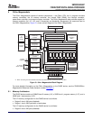
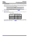
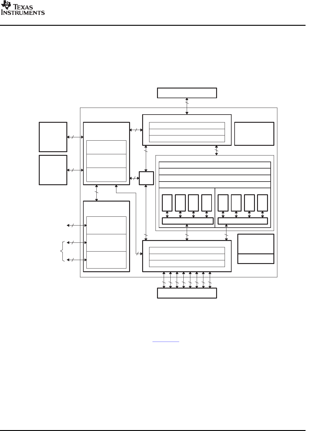
TheC64x+Megamoduleconsistsofseveralcomponents—theC64x+CPU,theL1programanddata
memorycontrollers,theL2memorycontroller,theinternalDMA(IDMA),theinterruptcontroller,
power-downcontroller,andexternalmemorycontroller.TheC64x+Megamodulealsoprovidessupportfor
memoryprotection(forL1P,L1D,andL2memories)andbandwidthmanagement(forresourceslocalto
theC64x+Megamodule).Figure5-1showsablockdiagramoftheC64x+Megamodule.
Figure5-1.64x+MegamoduleBlockDiagram
FormoredetailedinformationontheC64x+MegamoduleontheC6455device,seetheTMS320C64x+
MegamoduleReferenceGuide(literaturenumberSPRU871).
TheC6455devicecontainsa2096KBlevel-2memory(L2),a32KBlevel-1programmemory(L1P),anda
32KBlevel-1datamemory(L1D).
TheL1PmemoryconfigurationfortheC6455deviceisasfollows:
•Region0sizeis0Kbytes(disabled).
•Region1sizeis32Kbyteswithnowaitstates.
TheL1DmemoryconfigurationfortheC6455deviceisasfollows:
•Region0sizeis0Kbytes(disabled).
SubmitDocumentationFeedbackC64x+Megamodule87