21555 Non-Transparent PCI-to-PCI Bridge User Manual 121
List of Registers
List of Registers 16
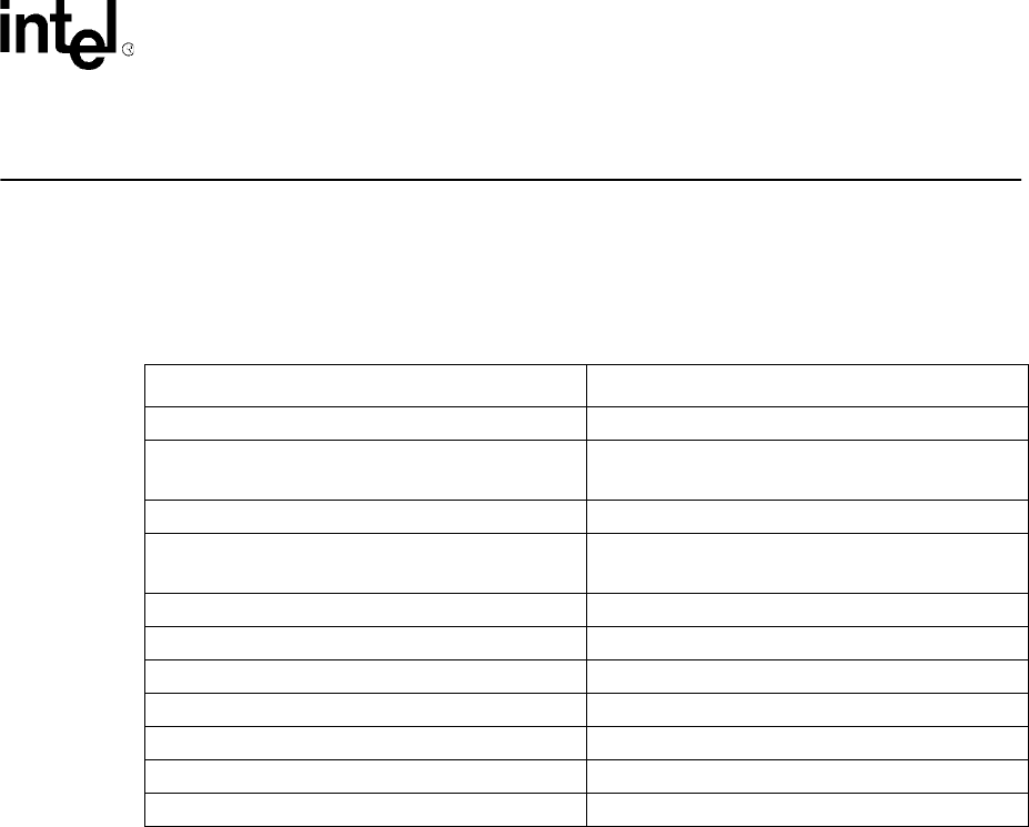
This chapter contains reference information about all of the 21555 registers. Table 31 is a cross reference between
the sections in this chapter to there accompanying theory of operation chapters.
16.1 Register Summary
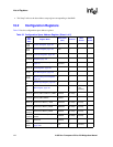
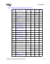
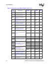
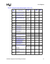
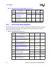
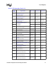
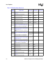
This chapter lists the 21555 configuration space registers and the CSR address map registers. A description of the
notes used in the tables used in this chapter are listed as follows:
• Byte offsets that are specific to the primary or secondary interfaces are followed by a (P) or (S) respectively.
All other byte offsets refer to both the primary and secondary address spaces. The configuration registers are
listed in order of primary byte offset.
• For read and write access, the following apply:
— Y: accessible from both primary and secondary interface.
— N: not accessible from either interface.
— Primary: for writes, only write from primary interface; for reads, reads as 0 from secondary interface.
— Secondary: for writes, only write from secondary interface; for reads, reads as 0 from primary interface.
— Special cases (for example, W1TC, W1TS, and R0TS) are noted.
• Some registers contain fields or bits with different access types (for example, R, R/W, W1TC) which are not
detailed in this table. See the individual register description for detailed information.
• Not all bits in every register denoted as preloadable are necessarily preloaded. See the individual register
description for detailed information.
Table 31. Register Cross Reference Table
Theory of Operation Chapter Register Reference Information.
Chapter 4, “Address Decoding” Section 16.4, “Address Decoding” on page 130
Chapter 3, “Signal Descriptions”
Chapter 5, “PCI Bus Transactions”
Section 16.5, “PCI Registers” on page 147
Chapter 6, “Initialization Requirements” Section 16.13, “Init Registers” on page 185
Chapter 11, “Interrupt and Scratchpad Registers”
Section 16.7, “Interrupt Registers” on page 170
Section 16.8, “Scratchpad Registers” on page 174
Chapter 8, “Parallel ROM Interface” Section 16.9, “PROM Registers” on page 175
Chapter 9, “Serial ROM Interface” Section 16.10, “SROM Registers” on page 179
Chapter 10, “Arbitration” Section 16.11, “Arbiter Control” on page 183
Chapter 12, “Error Handling” Section 16.12, “Error Registers” on page 183
Chapter 13, “JTAG Test Port” Section 16.14, “JTAG Registers” on page 190
Chapter 14, “I2O Support” Section 16.6, “I2O Registers” on page 165
Chapter 15, “VPD Support” Section 16.15, “VPD Registers” on page 192


