124 21555 Non-Transparent PCI-to-PCI Bridge User Manual
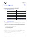
List of Registers
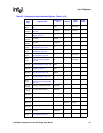
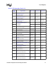
7D (P)
3D (S)
Primary and Secondary Interrupt
Pin Registers, page 155
00 — NY
7E (P)
3E (S)
Primary and Secondary Minimum
Grant Registers, page 155
00 Y N Y
7F (P)
3F (S)
Primary and Secondary
Maximum Latency Registers,
page 155
00 Y N Y
83:80
Downstream and Upstream
Configuration Address Registers,
page 141
Indeterminate — Primary Y
87:84
Downstream Configuration Data
and Upstream Configuration
Data Registers, page 142
Indeterminate — Primary Primary
8B:88
Downstream and Upstream
Configuration Address Registers,
page 141
Indeterminate — Secondary Y
8F:8C
Downstream Configuration Data
and Upstream Configuration
Data Registers, page 142
Indeterminate — Secondary
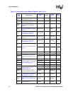
Second
ary
90
Configuration Own Bits Register,
page 142
00 — N
Primary
Read-0-
to- set
91 00 — N
Second
ary
Read-0-
to- set
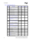
92:93 Configuration CSR, page 143 0000 — YY
9B:98 Downstream I/O or Memory 1
and Upstream I/O or Memory 0
Translated Base Register, page
136
Indeterminate — YY
A7:A4 Indeterminate — YY
97:94
Downstream Memory 0, 2, 3, and
Upstream Memory 1 Translated
Base Register, page 137
Indeterminate — YY
9F:9C Indeterminate — YY
A3:A0 Indeterminate — YY
AB:A8 Indeterminate — YY
AF:AC Downstream Memory 0, 2, 3, and
Upstream Memory 1 Setup
Registers, page 139
Downstream Memory 2 Setup
Downstream Memory 3 Setup
FFFFF000 Y Secondary Y
B7:B4 00000000 Y Secondary Y
BB:B8 00000000 Y Secondary Y
B3:B0
Downstream I/O or Memory 1
and Upstream I/O or Memory 0
Setup Registers, page 138
00000000 Y Secondary Y
BF:BC
Upper 32 Bits Downstream
Memory 3 Setup Register, page
140
00000000 Y Secondary Y
C3:C0
Primary Expansion ROM Setup
Register, page 176
00000000 Y Secondary Y
Table 32. Configuration Space Address Register (Sheet 3 of 5)
Byte
Offset
(Hex)
Register Name
Reset Value
(Hex)
Preload
Write
Access
Read
Access


