21555 Non-Transparent PCI-to-PCI Bridge User Manual 175
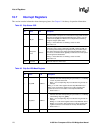
List of Registers
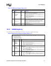
16.9 PROM Registers
This section describes the six PROM registers. See Chapter 8 for theory of operation information.
.
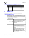
31:0 SCRATCH3 R/W 0B7:0B4h 32-bit scratchpad register 3.
31:0 SCRATCH4 R/W 0BB:0B8h 32-bit scratchpad register 4.
31:0 SCRATCH5 R/W 0BF:0BCh 32-bit scratchpad register 5.
31:0 SCRATCH6 R/W 0C3:0C0h 32-bit scratchpad register 6.
31:0 SCRATCH7 R/W 0C7:0C4h 32-bit scratchpad register 7.
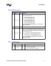
Table 107. Primary Expansion ROM BAR
This register defines an address range in which a memory read transaction on the primary interface of the
21555 results in a read access to the PROM interface. The Primary Expansion ROM Setup register controls
the size of the address range requested by the Primary Expansion ROM Base Address register. The Primary
Expansion ROM Setup register must be loaded either from the serial ROM or by the local processor before
configuration software running on the host processor can access this register. Local processor access should
be completed before the Configuration Lockout flag is cleared.
• Primary byte offset: 33:30h
• Secondary byte offset: 73:70h
Bit Name R/W Description
0
Address Decode
Enable
R/W
Enables the 21555 to respond to accesses to its expansion ROM
space. When this BAR is disabled, this bit will return zero when read.
• When 1, the 21555 responds to memory accesses to expansion
ROM space when the Memory Enable bit is also set.
• When 0, the 21555 does not respond to accesses directed to this
address space.
• Reset value is 0.
11:1 Reserved R Reserved. Returns 0 when read.
31:12 Base Address R/W
These bits are used to indicate the size of the expansion ROM space
and to set the base address of the range. Bits [23:11] of the Primary
Expansion ROM Setup register determine the function of the
corresponding bit in this register.
• When a bit in the Primary Expansion ROM Setup register is 0, the
same bit in this register is a read
-only bit and always returns 0
when read.
• When a bit in the Primary Expansion ROM Setup register is 1, the
same bit in this register is writable and returns the value last
written when read.
• When this BAR is enabled, bits [31:24] are always writable.
Writing a zero to bit [24] of the Primary Expansion ROM Setup
register disables this BAR. The minimum size for this address
range is 4 KB. The maximum size is 16 MB.
• Reset value is 0 (disabled).
Table 106. Scratchpad 0 Through Scratchpad 7 Registers (Sheet 2 of 2)
Bit Name R/W Byte Offset: Description


