21555 Non-Transparent PCI-to-PCI Bridge User Manual 179
List of Registers
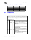
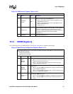
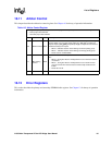
16.10 SROM Registers
This sections describes the SROM registers. See Chapter 9 for theory of operation information.
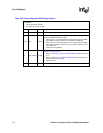
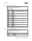
2
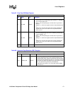
Read/Write
Control
R/W
PROM read/write control bit. This bit may be written with the same
CSR access that sets the PROM Start bit.
• When 0, the 21555 performs a read of the PROM when the
PROM Start bit is set to a 1.
• When 1, the 21555 performs a write of the PROM when the
PROM Start bit is set to a 1.
• Reset value is 0
3SROM_POLL R
This bit reflects the status of the serial ROM as a result of a polling
operation following a write all, erase all, write, or erase operation.
This bit is set automatically by the 21555 when one of these
operations is initiated, and cleared when a subsequent poll of the
serial ROM indicates that the operation is complete.
Reset value is 0
7:4 Reserved R Reserved. Reads only as 0.
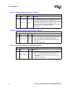
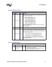
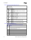
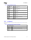
Table 113. Mode Setting Configuration Register (Sheet 1 of 2)
This register reflects the various mode settings selected by strapping the pr_ad pins, as well as whether the
64-bit extension is enabled.
• Primary byte offset: D6h
• Secondary byte offset: D6h
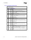
Bit Name R/W Description
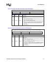
0
Serial
Preload
Enabled
R
Indicates whether a serial preload was performed.
• When 0, the serial preload enable sequence was not detected and the
register preload was not performed.
• When 1, the serial preload enable sequence was detected and the
register preload was performed.
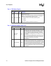
1
Primary
Lockout
Reset Value
R
Indicates the primary lockout reset value determined by sampling pr_ad[3]
during reset.
• When 0, signal pr_ad[3] was sampled low, causing the this bit to be low
upon completion of chip reset.
• When 1, signal pr_ad[3] was sampled high, causing the this bit to be set
high upon completion of chip reset.
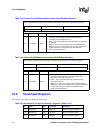
2
Synchronous
Enable
R
Indicates whether synchronous or asynchronous mode was selected by
sampling pr_ad[4] during reset.
• When 0, signal pr_ad[4] was sampled low, selecting synchronous mode.
• When 1, signal pr_ad[4] was sampled high, selecting asynchronous
mode.
Table 112. ROM Control Register (Sheet 2 of 2)
Byte Offsets: 0CFh
Bit Name R/W Description


