21555 Non-Transparent PCI-to-PCI Bridge User Manual 157
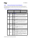
List of Registers
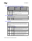
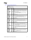
3
Secondary
Master
Timeout
R/W
Sets the maximum number of PCI clock cycles that the 21555 waits for an
initiator on the secondary bus to repeat a delayed transaction request. The
counter starts when the delayed transaction completion is ready to be
returned to the initiator. When the initiator has not repeated the transaction
at least once before the counter expires, the 21555 discards the delayed
transaction from its queues.
• When 0, the secondary master timeout counter is 2
15
PCI clock
cycles, or.983ms for a 33
-MHz bus.
• When 1, the value is 2
10
PCI clock cycles, or 30.7 µs for a 33-MHz
bus.
• Reset value is 0
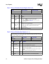
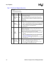
4
Primary
Master
Timeout
Disable
R/W
Disables the primary master timeout counter.
• When 0, the primary master timeout counter is enabled and uses the
value specified by the Primary Master timeout bit.
• When 1, the primary master timeout counter is disabled. The 21555
waits indefinitely for a primary bus initiator to repeat a delayed
transaction.
• Reset value is 0
5
Secondary
Master
Timeout
Disable
R/W
Disables the secondary master timeout counter.
• When 0, the secondary master timeout counter is enabled and uses
the value specified by the Secondary Master Timeout bit.
• When 1, the secondary master timeout counter is disabled. The 21555
waits indefinitely for a secondary bus initiator to repeat a delayed
transaction.
• Reset value is 0
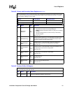
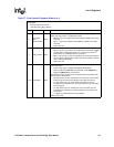
6
Delayed
Transaction
Order Control
R/W
Controls how the 21555 initiates delayed transactions on the target bus.
• When 0, the 21555 uses a round
-robin arbitration scheme to
determine which transaction is attempted. After receiving a target retry
in response to a delayed transaction, the 21555 can initiate a different
queued delayed transaction.
• When 1, When a target retry is received in response to a delayed
transaction, the 21555 continues to attempt that same transaction until
a response other than target retry is received. The 21555 does not
initiate other delayed transactions until the above condition is
satisfied.
• Reset value is 0.
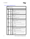
7
SERR#
Forward
Enable
R/W
SERR# forward enable.
When 0, the 21555 does not assert p_serr_l as a result of s_serr_l
assertion.
When 1, the 21555 asserts p_serr_l when s_serr_l is detected asserted
and the primary SERR# Enable bit is set.
Reset value is 0
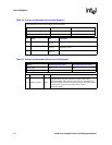
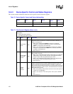
Table 77. Chip Control 0 Register (Sheet 2 of 4)
This register may be preloaded by serial ROM or programmed by the local processor before host
configuration.
• Primary byte offset: CD:CCh
• Secondary byte offset: CD:CCh
Bit Name R/W Description


